

Introduction
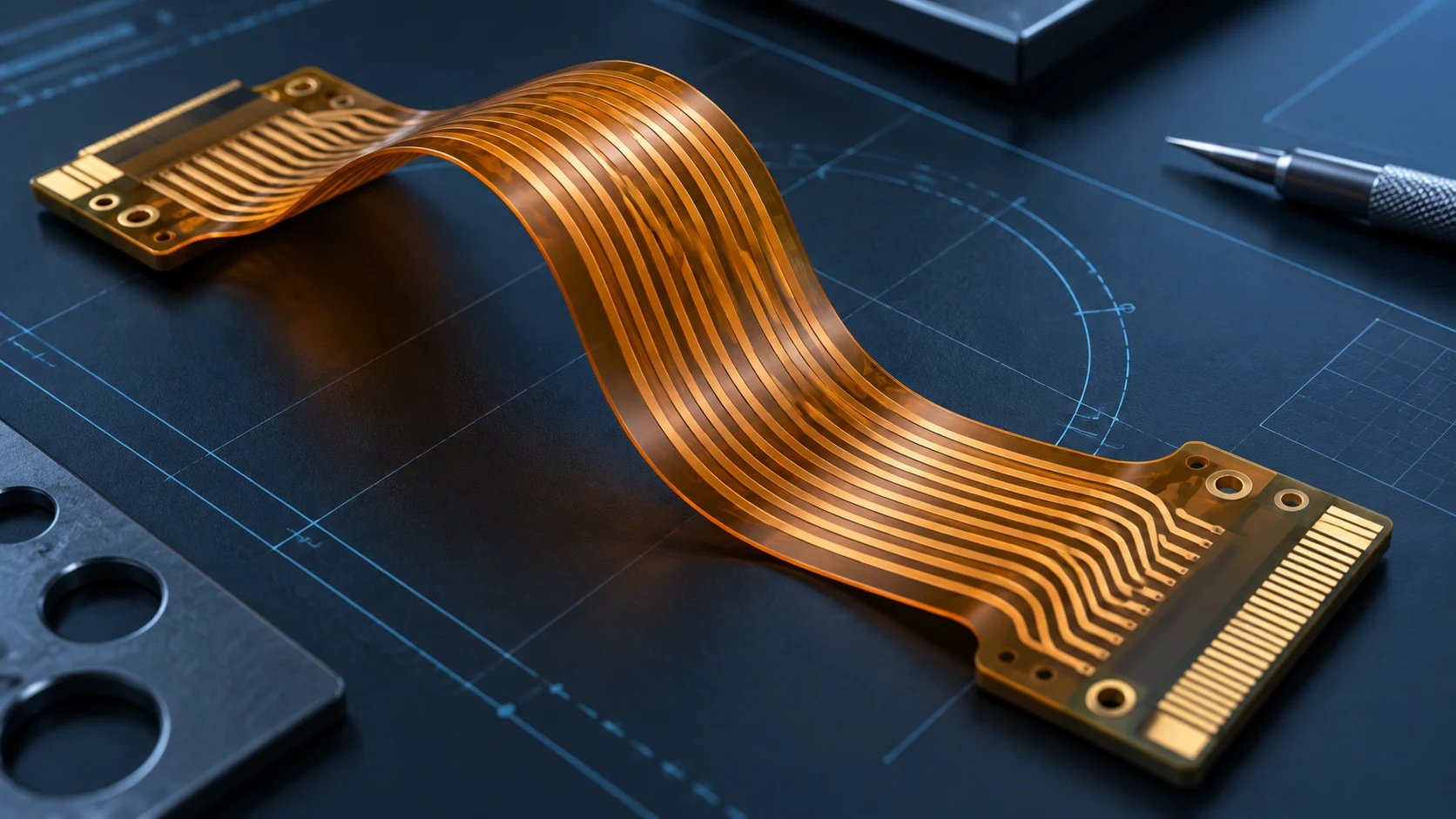
Flexible PCB materials are a system, not a single amber film selected from a catalogue. Copper, dielectric, adhesive, coverlay, plating and local stiffeners work together in the finished circuit. A change to one layer can alter total thickness, bend behavior, dimensional stability, assembly temperature exposure and connector fit.
That is why an OEM should define material choices through the application and the approved stack-up. A wearable sensor, a fixed automotive display tail and a robot joint may all use polyimide flex, yet they do not create the same motion, electrical or assembly demands. The useful procurement question is not “Which material is best?” It is “Which documented construction fits this duty, and how will the prototype prove it?”
This guide gives hardware engineers and B2B buyers a practical sequence for comparing polyimide flex PCB constructions, adhesive and adhesiveless laminates, copper foil, coverlay and stiffeners. Use it with the broader flexible PCB design guidelines and the application-specific flex PCB bend radius guide before releasing an RFQ.
Start with the application before naming a material
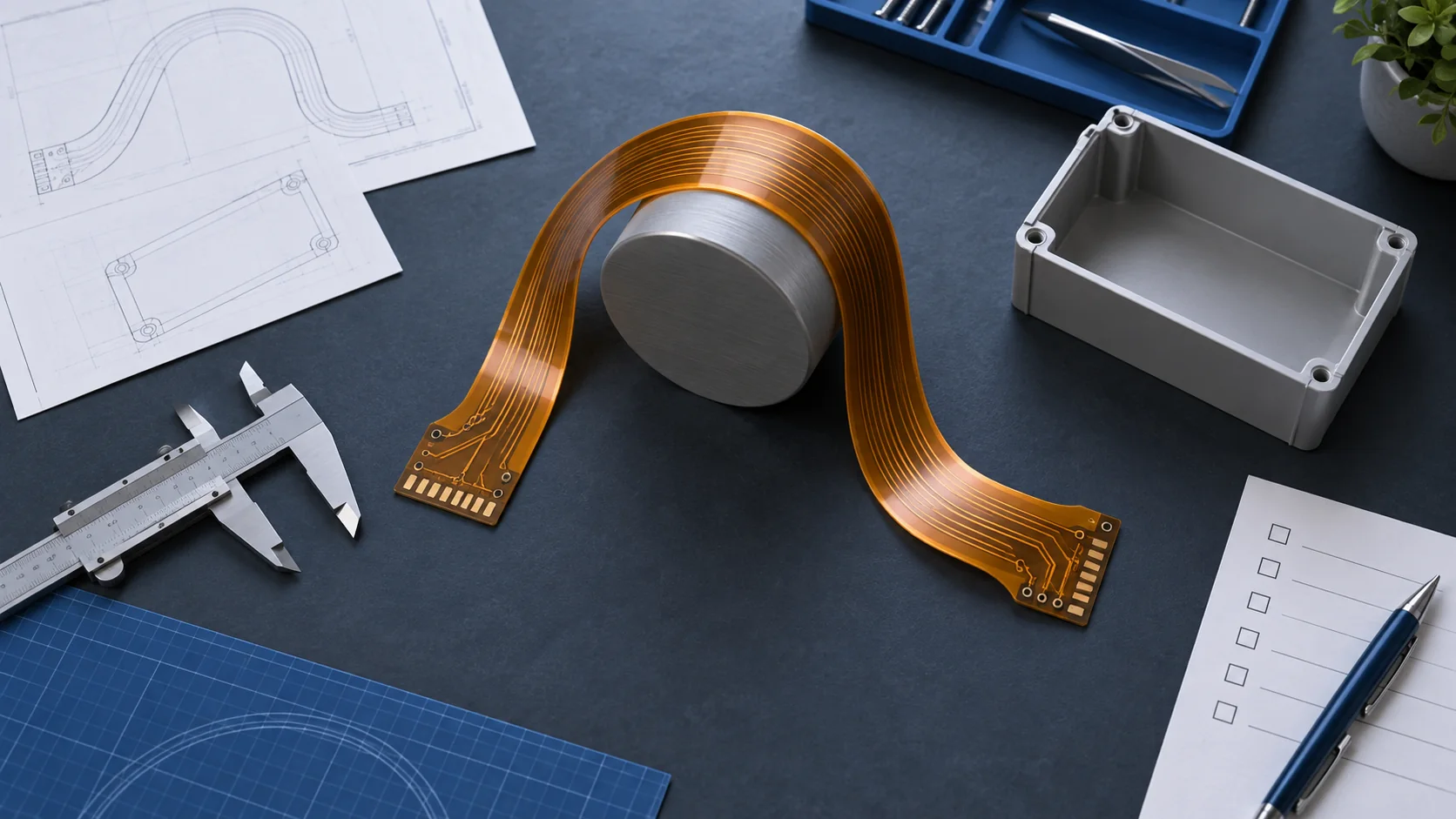
Begin with the installed product. State whether each flexible region is formed once, adjusted during service or moved continuously. Record the available envelope, minimum observed radius, torsion, contact with nearby parts, temperature range, humidity or chemical exposure, electrical load, signal requirements and assembly process. These inputs tell the supplier what the material system must do.
Separate mandatory product requirements from preferred construction details. “The tail must pass through this hinge for the validated product life” is a requirement. “Use a specific copper type and film thickness” may be a design choice that still needs confirmation. This distinction lets engineering teams compare alternatives without losing the reason behind the specification.
Also identify local zones. The moving span, connector land, component area and bonded stiffener do not need the same flexibility. A good drawing marks those zones and prevents a rigid feature from drifting into the active bend during revision. If the duty is not yet measured, treat the stack-up as provisional and build the measurement plan into the prototype phase.
Map the functional layers in the flex PCB stack-up
A material callout becomes useful when every layer has a function. The dielectric film provides insulation and a flexible carrier. Copper forms the conductors. An adhesive may bond copper to the dielectric or bond a coverlay to the etched circuit. Coverlay protects conductors while leaving pads and contacts exposed. Plating and surface finish support interconnection and assembly. Stiffeners add local support where a connector, component or contact area needs controlled thickness.
Do not reduce this map to “PI plus copper.” Two circuits with the same nominal polyimide thickness can behave differently because copper weight, plating, adhesive, coverlay and local reinforcement change the finished build. Ask for both nominal material thicknesses and the expected finished thickness in relevant zones. Connector interfaces should be checked against the final stack, not only the base laminate.
For multilayer flex or rigid-flex, include bondply, coverlay openings, via structures and any rigid sections in the same controlled drawing. The material family and supplier grade should be linked to an approved data sheet or an agreed equivalent. If equivalents are allowed, define which properties and qualification evidence must remain comparable before a substitution is accepted.
Compare adhesive-based and adhesiveless laminates
In an adhesive-based laminate, a bonding layer joins copper to the flexible dielectric. In an adhesiveless laminate, copper is bonded directly to an all-polyimide or comparable dielectric construction without that separate adhesive layer. Both approaches are established; the project determines which trade-offs matter.
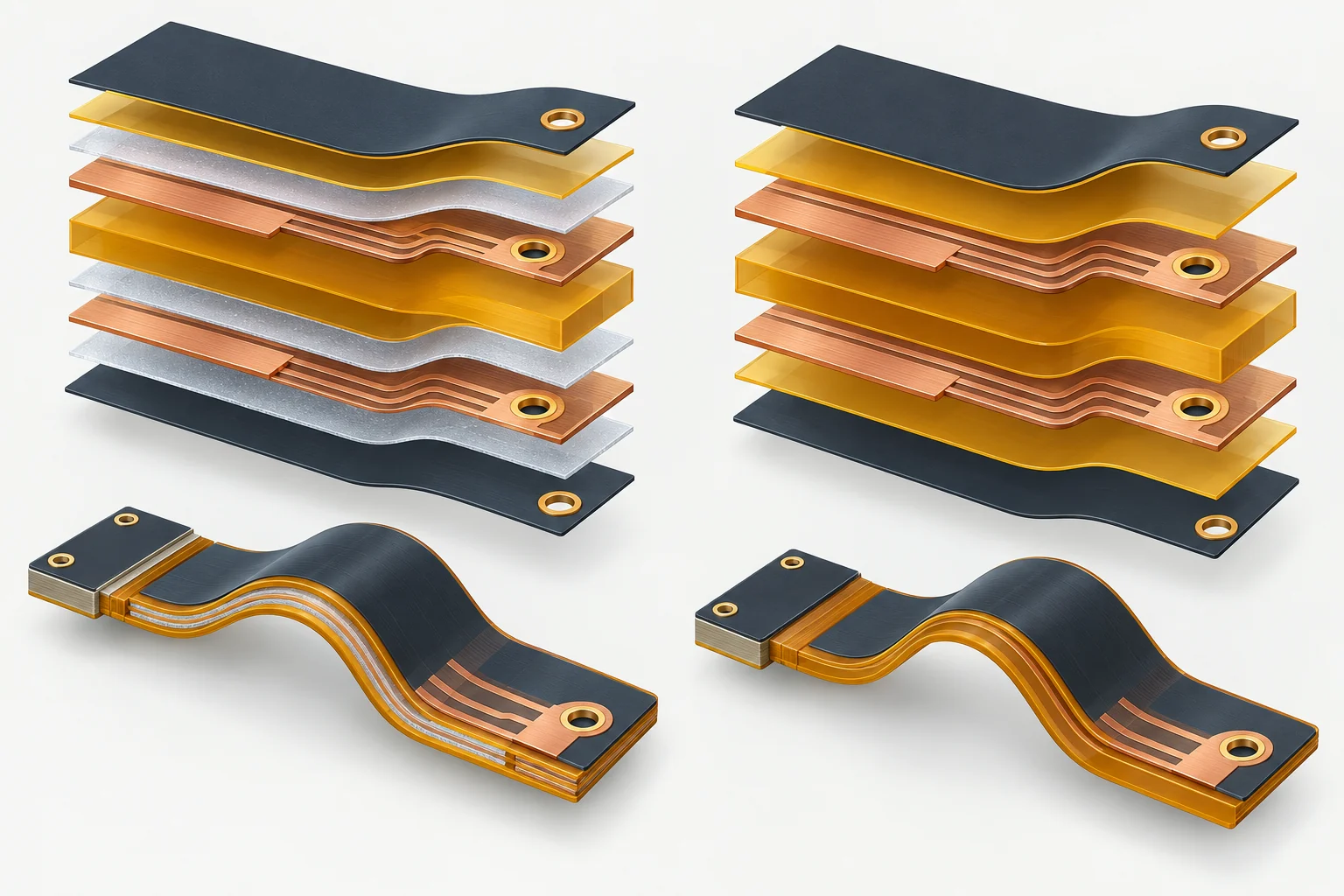
An adhesiveless core can reduce layer count and total thickness, which may help a compact build or a demanding bend. It can also simplify the dielectric system considered for electrical and thermal behavior. An adhesive-based construction may offer a practical, well-understood material route for many static or cost-sensitive designs. Neither label alone proves reliability, price or availability.
Review the exact laminate data sheet, processing window, dimensional behavior, peel performance and applicable recognition for the proposed grade. DuPont, for example, publishes distinct flexible laminate and adhesive-system families rather than one universal flex material. Treat published values as grade-specific test data, not as a blanket promise for the finished board. The fabricator should confirm the proposed construction and the OEM should validate it in the actual assembly.
Select copper foil for the actual bend duty
Copper selection affects electrical resistance, etching, thickness and fatigue behavior. Rolled annealed copper is commonly considered for repeated flexing because its processed grain structure can support ductility in the rolling direction. Electrodeposited copper is available in several profiles and treatments and may be appropriate for many fixed-flex and high-density constructions. The foil name alone does not determine the life of a circuit.
Evaluate copper type together with copper thickness, trace width, plating, grain direction where relevant, bend direction and local geometry. A plated area, via or abrupt width change inside a moving span can dominate strain even when the base foil is well chosen. Dynamic designs also need the mechanical path, loop length and support system defined; material selection cannot repair a pinched or creased installation.
Specify whether the drawing value describes starting foil, finished copper or minimum local copper after processing. Ask the supplier to identify the proposed foil family and any assumptions about plating. Then connect the stack-up to the bend drawing and prototype test. This creates a traceable basis for approval rather than a generic instruction such as “use flexible copper.”
Coordinate coverlay, openings, finish and stiffeners
Flex PCB coverlay protects the etched conductors and provides insulation, but its film and adhesive also add thickness and stiffness. Define coverlay film, adhesive, opening geometry and registration expectations where pads, fingers or components are exposed. Small webs, tight openings and transition edges should be reviewed for manufacturability before tooling.
A flexible PCB stiffener is a local mechanical element. Polyimide reinforcement may help build thickness while retaining a slim profile; FR-4 or metal reinforcement can provide greater local rigidity where the assembly requires it. State the stiffener material, thickness, outline, bonding method and tolerance, and keep its edge out of an active bend unless the transition is specifically engineered. Connector areas also need the finished insertion thickness and exposed-contact geometry checked together.
Surface finish belongs in the same interface review. Choose it from the assembly method, contact function, storage and qualification requirements. Avoid copying a finish from another product without checking the connector or bonding process. The supplier’s proposal should connect the finish, pad metallurgy, coverlay opening and assembly temperature exposure to one controlled revision.
Translate use cases into material decisions
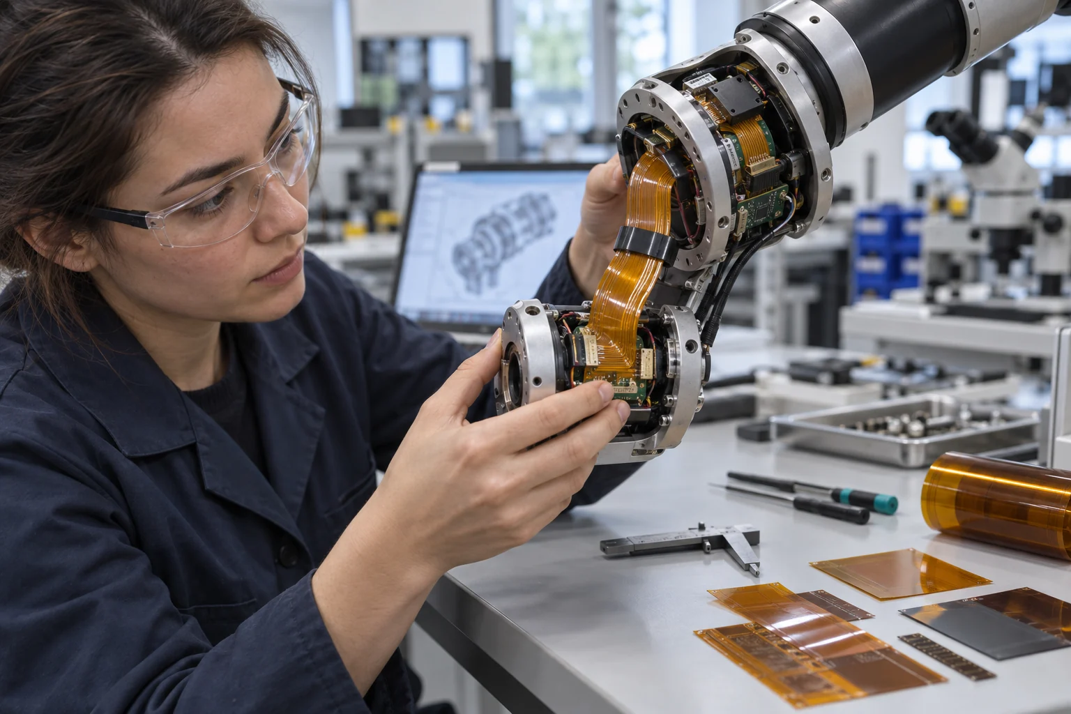
Use cases help organize questions, but they do not replace engineering validation. A moving robot joint emphasizes repeated motion, controlled routing and strain relief. A compact wearable emphasizes thickness, mass, body geometry and assembly interfaces. A curved display tail may be formed during installation and then remain static, placing more emphasis on connector geometry, dimensional control and the formed path.
| Use case | Material questions | Evidence to request |
|---|---|---|
| Robotic or articulated joint | Copper type and thickness, total build, coverlay, transition zones and motion path | Controlled stack-up, bend drawing, fixture description and cycle-test plan |
| Wearable or compact sensor | Thin construction, local stiffeners, connector fit, skin-side enclosure and assembly heat | Zone thicknesses, material data, assembly drawing and sample inspection criteria |
| Automotive or industrial display | Installed fold, thermal exposure, finish, coverlay openings and connector geometry | Formed-state drawing, environmental plan, interface dimensions and change control |
These examples match the decision paths shown in Teleconix application pages for a humanoid robotic joint FPC, a wearable display FPC and an automotive curved display FPC. Use those pages to frame the application, then submit the real mechanical and electrical constraints for project-specific review.
Build a controlled material stack-up and RFQ package
A useful RFQ lets the fabricator trace each decision to a requirement. Send fabrication data, a dimensioned outline, a layer and material stack-up, coverlay and stiffener drawings, connector specifications, surface-finish requirements, the formed-state or motion drawing, test expectations and the current revision. Flag any item that is a target rather than a released requirement.
| RFQ item | Buyer input | Supplier response expected |
|---|---|---|
| Application duty | Static, service or dynamic motion; environment; electrical load | Construction assumptions and unresolved risks |
| Material system | Required grade or performance basis; allowed equivalents | Proposed laminate, coverlay, adhesive and copper identification |
| Finished stack | Zone drawings and connector requirements | Nominal and controlled finished thickness by zone |
| Interfaces | Contacts, components, stiffeners and assembly process | Opening, finish, reinforcement and tolerance proposal |
| Validation | Acceptance criteria and product fixture | Coupon, sample, inspection and test plan |
| Change control | Approval level for substitutions | Traceability and notification method |
Ask the quotation to identify exclusions and open questions. A low price based on an assumed material is not comparable with a quote tied to a named construction and validation plan. For collaborative review, Teleconix’s OEM/ODM process provides the broader handoff context for drawings, samples and revisions.
Check electrical, thermal and environmental properties
Mechanical flexibility is only one part of the material decision. High-speed or impedance-controlled interconnects also depend on dielectric thickness, dielectric properties, copper profile, trace geometry and the surrounding stack. Power circuits add conductor temperature rise and thermal-path questions. Assemblies exposed to sustained heat, humidity, fluids or repeated thermal cycling need material data and qualification conditions that match the product risk.
Use supplier data sheets to build the shortlist, then check how the published test method relates to the finished circuit. A typical value measured on a laminate specimen is not the same as a guaranteed value for an etched, plated and assembled board. Frequency, temperature, conditioning, copper treatment and test geometry can change the meaning of a number. Where electrical performance is critical, define the model inputs, coupon or test structure, measurement method and acceptance band in the project plan.
Assembly exposure belongs in this review. Record the soldering or bonding process, peak and time profile, number of thermal excursions, cleaning chemistry and any later overmolding or adhesive cure. A material system that looks suitable in service can still be a poor fit for the chosen assembly sequence. Connector pads, fine-pitch bonding areas and component islands may each need separate interface checks.
For regulated or high-reliability products, list required declarations, recognition and qualification evidence explicitly. Do not infer flame, medical, automotive or environmental compliance from the word “polyimide.” Confirm the exact material grade, construction, finished-board requirement and applicable document revision with the responsible supplier and the OEM quality team.
Avoid common flexible PCB material specification errors
One common error is specifying only a brand family. Families contain multiple laminates, adhesives, coverlays and copper options, so the family name may not identify the build. Use a supplier grade or a performance-based definition with an approved-equivalent process. Another error is mixing nominal raw-material thickness with finished thickness at plated, covered or reinforced zones. Keep both values visible and state which one controls the interface.
Teams also reuse a stack-up from a visually similar product without transferring the actual duty. A display tail that bends once cannot justify a robot-joint construction, and a thin wearable design does not prove compatibility with an automotive thermal cycle. Preserve the application rationale with the stack-up so later revisions do not copy the layers while losing the boundary conditions.
A third error is treating the stiffener as an afterthought. Moving its edge, changing its adhesive or altering its thickness can affect connector engagement and concentrate strain. Include stiffeners in the controlled mechanical drawing and first-article inspection. The same rule applies to coverlay openings, plating zones and transitions between rigid and flexible areas.
Finally, avoid silent substitutions. Supply disruption may make an alternative reasonable, but approval should compare the properties that matter to the product and define the required evidence. Depending on the change, that may include a data-sheet review, dimensional sample, assembly trial, electrical test or repeated-motion validation. Recording this route before production gives purchasing a practical response to availability changes without bypassing engineering control.
Validate the prototype and control material changes
Prototype approval should connect the physical sample to the exact stack-up. Record the material family, copper basis, coverlay, adhesive or bondply, stiffeners, surface finish and relevant finished thicknesses. Inspect critical openings and transition zones, then assemble the flex in the intended housing or fixture before judging fit and bend behavior.
Test the failure modes created by the product. A dynamic assembly may need continuity monitoring through motion and inspection at defined intervals. A formed-static tail may need installation repeatability, connector retention and environmental exposure. An assembly with fine contacts may need interface-specific dimensional and electrical checks. The acceptance plan should state sample size, fixture, conditions, measurements and pass/fail criteria rather than relying on a visual bend demonstration.
After approval, protect the result with material traceability and change control. Define which substitutions require data review, a sample build or full requalification. The applicable IPC design and material families include IPC-2223 for flex and rigid-flex design and the IPC-4202, IPC-4203 and IPC-4204 material specifications listed in the IPC document revision table. State the revision and acceptance basis agreed for the project; do not assume that a standard number by itself defines the finished construction.
Related Products
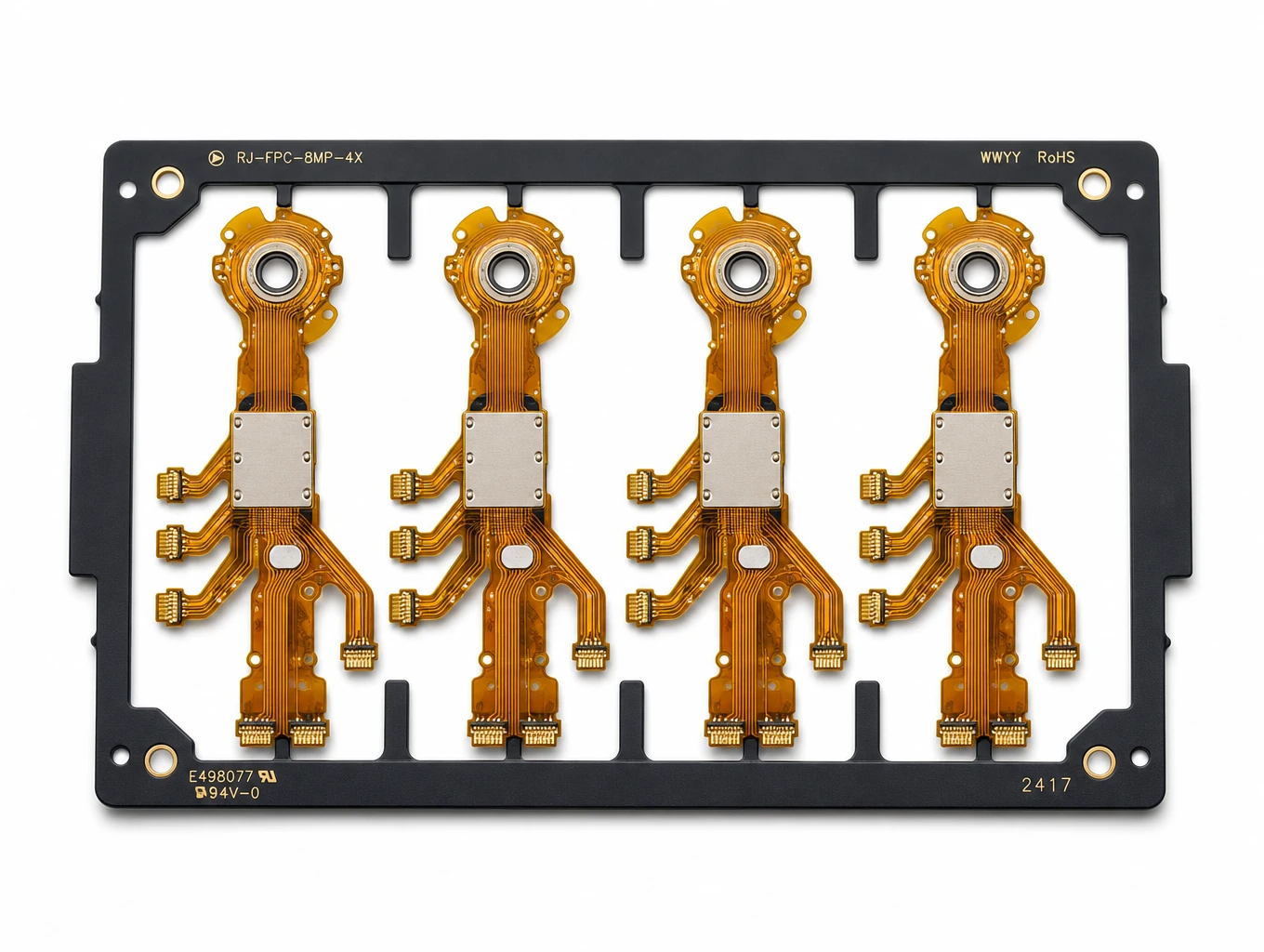
Multi-Branch Humanoid Robotic Joint FPC
Model: TLX-ROB-JNT01
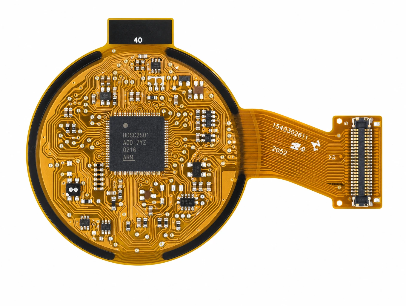
Wearable Smartwatch & Round AMOLED FPC
Model: TLX-DFPC-WEAR04
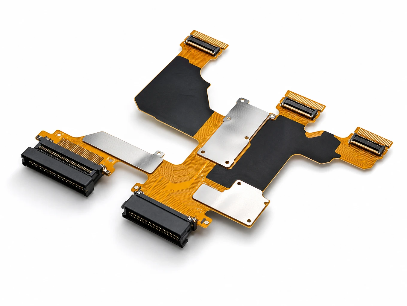
Automotive Curved Cockpit Display FPC
Model: TLX-DFPC-AUTO03
相关解决方案

AI & Robotics & Special Industrial FPC
Overcome severe mechanical stress and extreme spatial constraints in your automated hardware. We design and manufacture custom flexible circuits engineered to endure over 2 million continuous bending cycles in multi-axis robotic joints, bionic grippers, and autonomous AGV/AMR platforms.
Explore Solutions
Smart Automotive Electronics FPC
Teleconix delivers advanced flexible interconnects for ADAS, in-vehicle infotainment, powertrain control, and battery management systems — engineered for performance in intelligent automotive systems.
Explore Solutions
Display FPC
Teleconix manufactures fine-pitch, high-density FPCs for LCD, OLED, mini-LED displays, camera modules, and optical sensors — delivering stable signal transmission and exceptional brightness control.
Explore Solutions
AI & Robotics & Special Industrial FPC
Overcome severe mechanical stress and extreme spatial constraints in your automated hardware. We design and manufacture custom flexible circuits engineered to endure over 2 million continuous bending cycles in multi-axis robotic joints, bionic grippers, and autonomous AGV/AMR platforms.
Explore Solutions
Smart Automotive Electronics FPC
Teleconix delivers advanced flexible interconnects for ADAS, in-vehicle infotainment, powertrain control, and battery management systems — engineered for performance in intelligent automotive systems.
Explore Solutions
Display FPC
Teleconix manufactures fine-pitch, high-density FPCs for LCD, OLED, mini-LED displays, camera modules, and optical sensors — delivering stable signal transmission and exceptional brightness control.
Explore SolutionsFrequently Asked Questions
Conclusion: approve a material system, not a shorthand
Flexible PCB materials should be released as a documented system tied to the application. Define the motion and environment first, map every functional layer, compare adhesive and adhesiveless options using real grade data, and coordinate copper, coverlay, finish and stiffeners with the installed geometry.
Before production, approve the proposed stack-up through a representative prototype and record the evidence needed for future substitutions. To discuss a new build, send your fabrication data, formed-state or motion drawing, connector details, environment and acceptance targets through the Teleconix project inquiry form. The team can review the package and identify the material decisions that still need agreement before quotation.