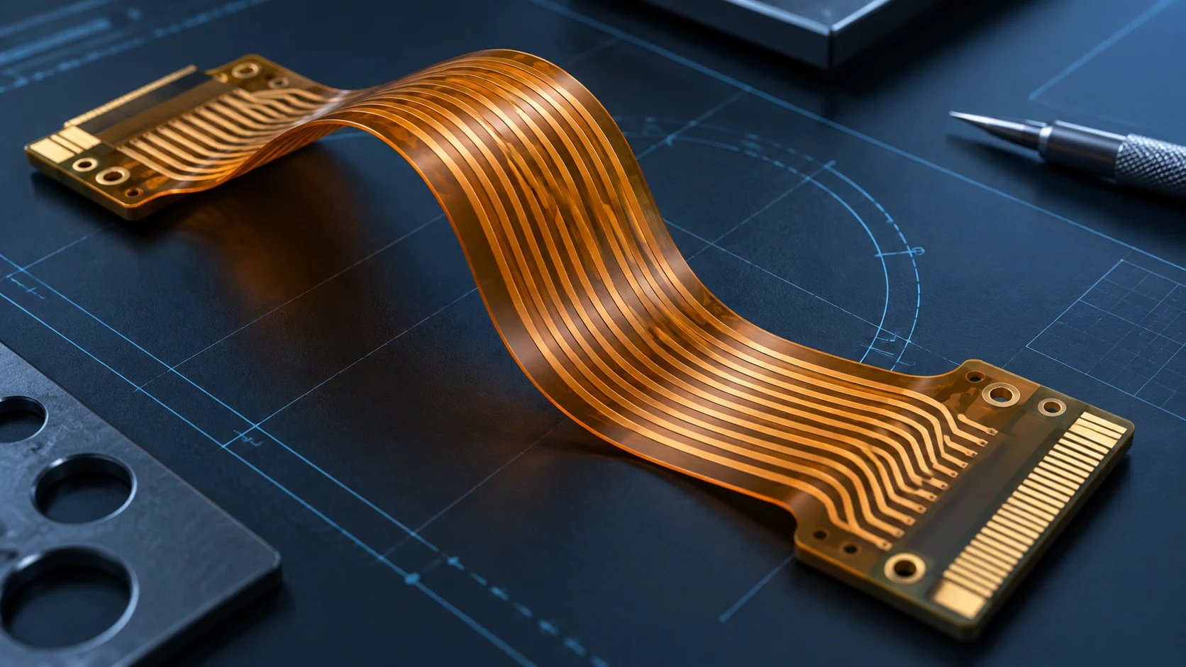

Controlled impedance flex PCB: start with the signal channel
Controlled impedance flex PCB design helps an OEM define a predictable transmission path through a flexible interconnect. The purchasing requirement must connect the intended interface, the physical construction and the verification method. A drawing that simply says “controlled impedance” leaves the manufacturer without a complete acceptance requirement and leaves the buyer without a clear way to compare quotations.
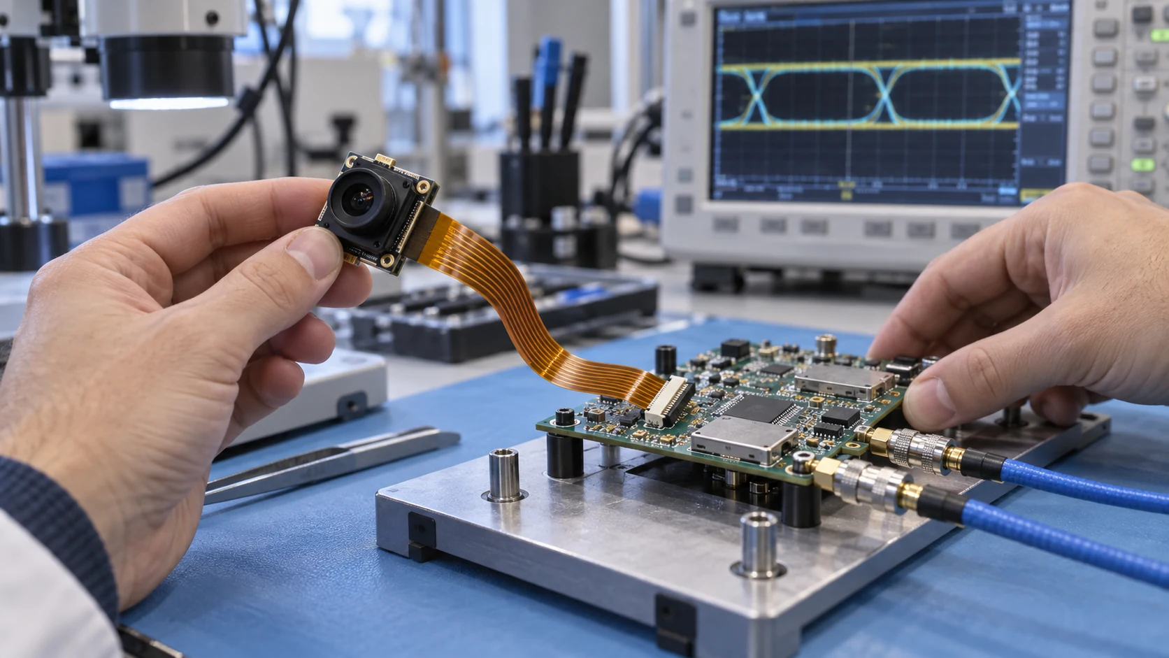
A camera, display or communication module may contain rigid boards, connectors and a flexible tail in the same channel. Review where the flex begins and ends, how it is installed and which signals require special attention. The relevant design includes the signal conductors and their return environment throughout the route, including transitions into supported areas.
This guide covers the OEM decisions to settle before layout release, prototype ordering and production approval. Use it alongside the flexible PCB design guidelines to turn electrical requirements into a consistent drawing, stack-up and RFQ package.
Define controlled impedance and the acceptance boundary
Characteristic impedance describes the relationship between voltage and current for a travelling wave along a transmission structure. It is different from the DC resistance measured along a copper trace. A circuit can pass continuity testing while still having a transmission path that differs from the intended electrical design.
For an impedance controlled flexible PCB, the drawing should identify the controlled nets, nominal target, permitted range and associated construction. It should also identify whether acceptance applies to a production coupon, the circuit itself or an assembled channel. These are related measurements, but they do not demonstrate the same thing.
Separate three approval questions: does the manufactured structure meet its agreed requirement, does the assembled interconnect maintain an acceptable channel, and does the complete product meet its interface specification? Assign an owner to each question. This prevents a fabrication report from being treated as evidence for a system test that nobody actually performed.
Use interface requirements to choose the target
Obtain impedance targets from the applicable interface specification and the component manufacturer’s current design guidance. Confirm the interface generation, operating conditions and channel definition. Commonly quoted values are useful examples in training, but choosing a familiar number without checking the application can create a mismatched requirement.
State whether each net is single-ended or part of a differential pair. Include the relevant reference layer and identify the pair members by their actual net names. If the design contains more than one structure or target, give each structure its own identifier in the drawing and test plan.
Signal edge rate, route length and the channel environment matter alongside the data rate. Ask the system engineer which paths require modelling and which margins are important. For a first quotation, unresolved targets should appear as open technical questions rather than as hidden assumptions that become expensive to change after layout.
Build the stack-up before freezing trace geometry
A trace width has meaning only within its surrounding structure. Record the conductor layer, intended reference, dielectric materials and thicknesses, copper construction and protective layers. Distinguish nominal incoming material thickness from the finished construction used in the impedance model. Ask the supplier which values it uses and how they relate to the released drawing.
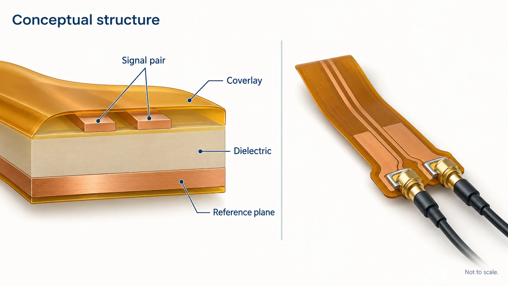
Review the actual flex cross-section instead of copying a rigid-board calculator example. A protective coverlay and its adhesive can be part of the electrical environment. Local openings, bonded layers and changes between rigid and flexible regions can create different cross-sections along one route. Identify those regions explicitly.
The flexible PCB materials guide explains the material choices to record in an RFQ. For impedance work, add the dielectric data and model assumptions relevant to the application. Approve the proposed stack-up before fixing layout rules, then carry its revision into fabrication and prototype records.
Record the inputs that influence impedance
The checklist below is a starting point for a technical discussion. It deliberately gives no universal trace width, dielectric constant or tolerance. The supplier and OEM should resolve the inputs for the actual structure and identify which dimensions may be adjusted during engineering review.
Keep these inputs together in a controlled stack-up or drawing note. A material description in one email and a trace dimension in an unrelated spreadsheet are difficult to reconcile when a later revision changes the construction. Record both the agreed value and the source of any model assumption.
| Input | OEM decision | Review evidence |
|---|---|---|
| Signal structure | Single-ended or differential, layer and reference | Named nets and cross-section identifier |
| Copper geometry | Width, pair spacing and finished thickness assumptions | Approved geometry and adjustment authority |
| Dielectric construction | Materials, thicknesses and protective layers | Controlled stack-up and modelling data |
| Return environment | Plane pattern, openings and transitions | Layout review and region-specific model |
| Acceptance | Target, tolerance and measurement boundary | Agreed coupon or circuit test plan |
| Change control | Permitted process adjustments and substitutions | Written approval and matching release revision |
Model differential pairs as coupled structures
A differential pair contains two conductors whose electrical behaviour depends on their geometry and environment. Treat the pair as a coupled structure. Record both trace widths and the spacing convention used in the drawing, since a centre-to-centre distance and an edge-to-edge gap describe different dimensions.
Review symmetry through connectors, neck-downs and transitions. Equal total length does not by itself establish equal electrical behaviour if the two conductors encounter different surroundings. Keep the relevant reference environment consistent and check whether local routing changes require a more detailed analysis.
Do not specify only a differential value when the interface review also needs other quantities. Ask the system engineer which measurements are required and how they will be reported. A clearly named structure and an agreed test mode make a report easier to interpret than a result labelled merely “impedance” with no explanation.
Preserve the return environment through the route
Inspect reference-plane continuity around the controlled signals, especially near openings, connector exits and layer changes. A copper feature that looks connected in a layout view may still force return current through an undesirable path. Review the signal route and its reference together, rather than checking the trace in isolation.
Flex designs sometimes use patterned copper to balance electrical and mechanical requirements. If a reference is hatched or otherwise interrupted, specify the pattern and include it in the relevant modelling discussion. Do not assume that a model for a solid plane represents a different pattern accurately. An apparently small artwork change can alter the structure being evaluated.
Texas Instruments discusses plane splits and return paths in its interface layout guidance. The useful design lesson is to inspect continuity and transitions deliberately. Its device-specific dimensions and electrical targets should not be copied into another interface without checking the applicable component documentation.
Resolve connector and rigid-flex transitions
A uniform flexible transmission line can connect to a nonuniform launch, connector pad field or rigid-board transition. Review those areas as part of the complete channel. A good coupon result for the long uniform section does not characterize every short feature at the ends of the circuit.
Identify neck-down regions, pad geometry, vias and any change in reference layer. Ask whether a simple cross-section model is sufficient or whether the system needs a more detailed model of the transition. Include connector information and the mating board arrangement so the reviewer can understand the physical boundary.
For a rigid-flex build, document each cross-section and the transition between them. The rigid region and flex region may use different materials and geometries while carrying the same signal pair. Review how the electrical structure changes through that boundary and keep its drawing notes consistent with the mechanical routing.
Review the installed shape and mechanical requirements
Electrical and mechanical reviews should use the same released construction. A stack-up chosen for a signal path also affects thickness and the ability to route the flex inside an enclosure. Identify installation bends, repeated movement, supported islands and contact with nearby conductive parts. Provide a dimensioned installation view where these conditions matter.
Use the flex PCB bend radius guide to define the actual bend conditions. A generic impedance model does not establish a flexing lifetime, and a successful flat-circuit measurement does not by itself approve every installed configuration. Decide which mechanical conditions need representative prototype verification.
Agree when measurements will be made and how the sample will be held. If the installed position or repeated motion is part of qualification, describe it in the test plan. This makes electrical and mechanical acceptance compatible and prevents a test fixture from becoming an undocumented substitute for the real application.
Compare modelling assumptions with fabrication limits
Use a solver or calculation method that represents the proposed structure and supports the level of analysis needed. Record the model version, cross-section and input data. The resulting geometry is a design proposal that still needs fabrication review, including whether the dimensions can be produced consistently for the planned construction.
Ask the supplier how it accounts for the finished conductor profile, dielectric variation and other relevant process effects. Agree which artwork adjustments may be proposed to meet the electrical target. These adjustments should be reviewed before release, with special attention to pad interfaces, clearances and bend-related features.
Avoid treating a nominal simulation result as a production guarantee. A useful review explains the assumptions, practical manufacturing range and verification plan. Procurement can then compare suppliers on the same technical boundary instead of comparing a carefully qualified quotation with an unexplained tolerance claim.
Plan coupons and sampling before the prototype order
An impedance coupon is a test structure associated with a manufactured panel or lot. Decide which controlled structures it represents, where it is placed and how it relates to the production circuits. Ask the supplier to identify the relevant layer, geometry and construction for each coupon result.
Define the sampling plan and the records delivered with the lot. Include the coupon identifier, circuit revision and lot reference so a result can be traced to the shipment. If the application requires measurements on the actual circuit, discuss access and fixtures before ordering. Testing may need a design feature or sample arrangement that cannot be added conveniently after manufacture.
The flexible PCB prototype guide provides a broader first-article checklist. For controlled impedance, add the approved model, test structure and measurement agreement to that package. A prototype order should resolve these technical questions before the same design enters repeat production.
Understand what a TDR report demonstrates
Time-domain reflectometry, or TDR, uses reflections to examine changes along a transmission path. The technique can support impedance evaluation and help identify discontinuities. Ask for the test setup, measurement mode and the portion of the structure used for acceptance, so the plotted result has a defined meaning.
Tektronix explains that probing, connections, measurement procedure and instrument condition affect repeatability. Record the relevant setup and calibration information in the agreed method. A waveform without fixture context can be difficult to compare with a later measurement performed through a different connection.
A TDR result answers a specific measurement question. It does not replace every loss, crosstalk or functional assessment needed by the product. Define additional channel or system checks with the responsible engineer, and keep them separate from the fabrication acceptance report. The conceptual illustration below shows structure and test access without representing measured performance.
Keep electrical continuity and channel qualification separate
Continuity and isolation tests check for opens, shorts and related connectivity issues under the selected method. Impedance evaluation examines the transmission structure. Channel qualification can also involve frequency-dependent behaviour and interface-specific measurements. List these requirements separately in the RFQ so that the quoted test scope is unambiguous.
Decide who owns each test. A fabricator may supply circuit-level evidence while the OEM validates the assembled module and complete product. If a third party performs a measurement, record its role and the required report. Ensure that the quotation includes the requested work instead of assuming every item is part of a standard shipment.
For a communication or RF design, review the operating band, connections and complete channel with the system engineer. Impedance control is one part of that review. The acceptance plan should address the actual performance requirement rather than using a single nominal impedance result as a broad claim of signal integrity.
Release an RFQ that supports comparable quotations
Supply controlled fabrication data, the dimensioned drawing and the approved stack-up. Include a table of controlled nets and structures, target ranges, relevant reference layers and the agreed test scope. State quantity, prototype milestones, required reports and the authority for technical changes.
Review the FPC manufacturing process alongside this electrical checklist. It helps connect drawing requirements to production and inspection stages. If assembly is included, use the FPC assembly guide to clarify component sourcing, support and inspection responsibilities.
Ask each supplier to return exceptions and assumptions in writing. Compare the same construction, measurement boundary and records before comparing price. If a quotation proposes a different stack-up, treat it as a technical alternative requiring review. Do not mix its price with the baseline requirement while leaving the design change unrecorded.
Approve the first article and control later changes
Match the delivered circuit, stack-up revision, coupon report and drawing before approving the first article. Review any permitted geometry adjustments and confirm that the final data reflects the accepted build. Investigate a result outside the agreed range through a documented technical disposition rather than accepting an unexplained screenshot.
Use representative samples for the installed channel and any required mechanical or functional checks. Record which evidence supports fabrication acceptance and which supports product qualification. Approval should identify the tested configuration so a later team can determine whether a new connector, material or routing revision still falls within that evidence.
For repeat orders, define the notification and approval process for changes that may affect the controlled structure. Preserve lot references and agreed measurement records. A useful production handoff gives engineering and procurement the same baseline, allowing future quotations and revisions to be assessed against an identifiable accepted construction.
Technical references: Polar Instruments stack-up examples; Tektronix TDR measurement guidance; Texas Instruments interface layout guidance; Texas Instruments differential-pair transition review. These references explain engineering methods. They do not certify Teleconix equipment, tolerance or product performance.
Related Products
High-Speed AI Vision & LiDAR Sensor Matrix FPC
Model: TLX-AI-VIS02
High-Speed ADAS Multi-Camera SerDes FPC
Model: TLX-AUTO-ADAS02
400G/800G High-Speed Optical Transceiver Multi-Layer Flex PCB
Model: TLX-COMM-OPT03
Related Solutions

RF & Communication FPC Solutions
Custom RF flexible PCB and telecom interconnects for antenna modules, wireless terminals and high-speed communication assemblies. Coordinate materials, signal paths, shielding and connector support with Teleconix before prototype release.
Explore Solutions
Display FPC
Teleconix manufactures fine-pitch, high-density FPCs for LCD, OLED, mini-LED displays, camera modules, and optical sensors — delivering stable signal transmission and exceptional brightness control.
Explore Solutions
Consumer Electronics & Smart Card FPC Solutions
Custom flexible circuits for smart cards, TWS earbuds and compact wearables. Align routing, stack-up, component interfaces and prototype acceptance with Teleconix before releasing your OEM design.
Explore Solutions RF & Communication FPC Solutions
Custom RF flexible PCB and telecom interconnects for antenna modules, wireless terminals and high-speed communication assemblies. Coordinate materials, signal paths, shielding and connector support with Teleconix before prototype release.
Explore Solutions Display FPC
Teleconix manufactures fine-pitch, high-density FPCs for LCD, OLED, mini-LED displays, camera modules, and optical sensors — delivering stable signal transmission and exceptional brightness control.
Explore Solutions Consumer Electronics & Smart Card FPC Solutions
Custom flexible circuits for smart cards, TWS earbuds and compact wearables. Align routing, stack-up, component interfaces and prototype acceptance with Teleconix before releasing your OEM design.
Explore SolutionsFrequently Asked Questions
Discuss your controlled impedance flex PCB requirement
An effective controlled impedance flex PCB RFQ connects interface requirements, an approved construction and an agreed verification plan. Resolve the signal structure, return environment and test boundary before layout release, then qualify the installed channel with evidence appropriate to the product.
For communication, imaging or compact electronics projects, review Teleconix’s RF and communication FPC solutions. Send your stack-up, controlled nets, installation drawing and requested acceptance records through the contact page to discuss the project. Confirm the proposed construction and test scope during the technical review.