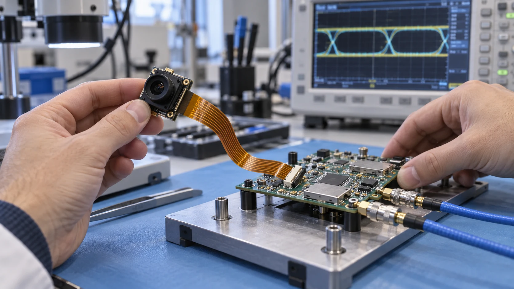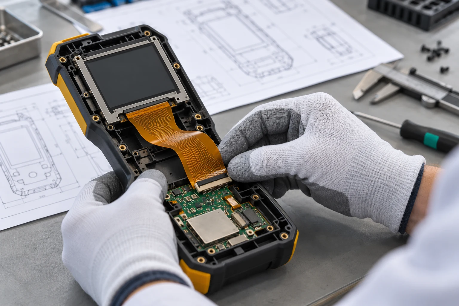


Telecom flexible PCB planning starts with the complete link
A telecom flexible PCB is a flexible printed circuit used within communication equipment to connect modules, carry signals or implement an antenna function. An OEM specification should identify exactly which role it serves. A radio feed, a digital data link and a radiating antenna need different design inputs and acceptance evidence.
Consider a compact wireless gateway. Its processor board, radio module, antenna and user interface may occupy different parts of the enclosure. The flexible circuit must connect the intended functions while fitting around supports, shields and assembly access. Electrical and mechanical decisions therefore belong in the same review before artwork release.
This guide turns those decisions into a practical handover for engineering and purchasing. Start with the communication terminal FPC product category for relevant configurations, then confirm the proposed construction against your own interface requirements. Product labels such as high-speed or RF do not establish a guaranteed channel performance for a different device.
Which functions belong on the communication flexible PCB?
Draw a block diagram showing every connected module and the boundary of the supplied FPC. Identify whether the supplier delivers a bare circuit, a connectorised interconnect or a populated assembly. Separate fabrication from integration work such as antenna tuning, firmware configuration and complete-device testing.
For a handheld terminal, the display connection may sit beside a radio path without carrying the same signal type. For an optical transceiver, the internal flexible link carries electrical signals between subassemblies even though the finished module communicates optically. Describe the actual nets and interfaces instead of treating all communication hardware as one RF application.
Allocate responsibilities early. The OEM should identify interface requirements and system acceptance; the fabricator should review the proposed construction and manufacturing constraints within its agreed scope. List any external laboratory or connector supplier involved. Record unresolved responsibilities beside the quotation so they cannot disappear between sample ordering and production release.
As a planning example, imagine that the gateway team moves the radio board to make room for a larger battery. The new flex route now crosses a mounting post, and the antenna attachment position also moves. Treat these as separate open decisions: mechanical engineering approves the route, the interface owner reviews the changed link, and the antenna owner evaluates the new surroundings. Purchasing then requests samples against that coordinated revision, rather than ordering the earlier outline with an informal instruction to make it longer.
Separate RF feedlines, data links and antenna elements
An RF flexible PCB may convey energy to an antenna, carry circuitry near a radio module, or form part of the antenna itself. Clarify that distinction on the drawing. A feedline normally aims to deliver a signal through a defined path; an antenna intentionally couples energy into or from its surroundings.
Use the following matrix to connect each function to the evidence needed. Several rows may apply to one assembly, but they should retain separate requirements. A successful check on one part of the link does not automatically validate the others.
| Function | OEM inputs | Review evidence |
|---|---|---|
| RF feed interconnect | Operating band, ports, reference paths and allowed channel losses | Agreed transmission and reflection checks with defined fixtures |
| High-speed digital link | Interface, lane mapping, channel budget and endpoint requirements | Channel assessment and applicable installed functional tests |
| Flexible antenna element | Radio design, enclosure, ground relationship and placement | Tuning and relevant radiated performance in the intended assembly |
| Power or low-speed control | Loads, voltage drop, sequencing and neighbouring circuits | Connection, load and functional checks for the specified duty |
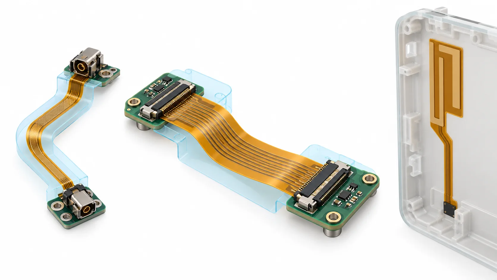
Define the interface before choosing an impedance target
Specify the actual radio or digital interface, connector part numbers and relevant component documentation. Record the operating band or data mode, single-ended or differential topology, pin assignment and permitted channel length where required. Targets should come from the selected system architecture rather than a generic flexible-circuit specification.
A transmission-line impedance target is one requirement within a larger channel budget. The path also includes connector transitions, board launches and the receiving interface. Ask which portions are included in the proposed analysis or measurement and where the reference planes are located. Agree the limits and reporting method before samples are built.
The controlled impedance flex PCB planning guide covers stack-up and coupon questions in more detail. For this telecom review, add the complete port-to-port boundary and system owner. Do not transfer an impedance tolerance or frequency claim from another product listing without confirmation for the proposed construction.
Review return paths and transitions as part of the channel
A route review should follow the signal and its reference connection through the entire assembly. Identify changes at connector tails, rigid-to-flex boundaries, vias and shield terminations. Put these features on the review drawing so the electrical designer and supplier can discuss them together with the installed geometry.
Texas Instruments’ High-Speed Interface Layout Guidelines recommends routing the covered high-speed signals over continuous ground references and explains the problems caused by crossing plane splits. This is a useful review principle, but the document’s particular routing recommendations are not a universal stack-up recipe for every flexible circuit.
For a flex assembly, document the proposed reference structure, local changes and connection to each mating board. Resolve trade-offs between electrical behaviour and mechanical flexibility with the responsible designers. Keep approved geometry and reference details in the controlled file set, especially when a connector or reinforcement boundary changes during packaging work.
Choose materials using the proposed telecom stack-up
Review dielectric, copper, protective layers, adhesives and reinforcement as one construction. Ask for the material information relevant to the operating conditions and design method. A familiar substrate name alone does not define the losses, dimensions or mechanical behaviour of the completed interconnect.
Where a project considers polyimide, LCP or another material system, compare proposals using the same channel boundary and sample requirements. Identify the actual grade, finished layer arrangement and manufacturing assumptions. Avoid selecting a material simply because it appears in a product title or is associated with a newer wireless generation.
Use the flexible PCB materials selection guide to organise the broader discussion. Request supplier confirmation of availability, process suitability and required evidence for your stack-up. Record permitted substitutions and the checks that a change would reopen; procurement should not treat similar nominal thicknesses as automatic electrical equivalence.
Reserve antenna space in the final enclosure
An antenna FPC needs a defined location and surrounding environment as well as an outline. Provide enclosure materials, nearby metalwork, batteries, shields and intended mounting. Assign the antenna designer responsibility for keep-out requirements and tuning rather than asking the fabricator to infer them from a drawing.
TI’s Antenna Selection Guide shows how the casing and nearby body can change antenna measurements, and recommends characterisation in the intended environment. Its short-range reference designs illustrate the principle; they do not establish an antenna design or pass limit for a different telecom terminal.
Plan access for tuning and identify which configuration represents the product. If a cover, adhesive or mounting position changes, ask the antenna owner which measurements need repeating. Keep this responsibility distinct from bare-board continuity testing. The RF and communication FPC solution provides an application starting point for discussing the delivered circuit and integration needs.
Define the installed route and any recurring movement
Supply three-dimensional views of the installed circuit, including intermediate assembly positions. Mark fixed supports, allowable route space, enclosure edges and connector access. A flexible link can fit the open housing yet become pinched, stretched or sharply folded when the cover and adjacent modules are installed.
Classify each region as an installation bend, service movement or recurring operating motion. A folding terminal hinge requires a different review from a stationary link inside a gateway. Define the motion path and relevant conditions, then agree a construction and prototype plan that address that duty.
The static and dynamic flex bend guide explains the information needed for this discussion. No universal bend radius or service life follows from the word flexible. For moving radio assemblies, consider both connection integrity and the system functions that must remain acceptable across the required positions and exposure sequence.
Control connector fit and support before ordering samples
State complete mating part numbers, contact side, pin mapping, insertion direction and finished tail requirements. Include the reinforcement and adhesive in the local thickness review. Confirm that the assembly sequence leaves room to engage the latch, inspect the connection and support the circuit without loading sensitive components.
Use the FPC stiffener and connector support checklist to define reinforcement boundaries. Review how the flexible span leaves the supported area and whether a housing feature imposes bending at that edge. Provide representative mating parts or controlled drawings for fit evaluation.
Separate a mechanical mating check from electrical channel approval. Matching pitch and insertion depth do not establish high-speed or RF suitability. Ask the interface owner to approve the connector selection, grounding arrangement and any required performance data. Include handling, permitted rework and replacement access in the assembly instructions.
Keep RF coexistence and power paths in the system review
A compact communication terminal may contain several radios, a display, charging circuitry and switching power supplies. Provide their positions and relevant operating states to the system designer. The flex drawing should identify which nets carry sensitive signals and which routes share nearby space or references.
Build a representative operating matrix instead of validating only one quiet laboratory state. For example, an OEM may need to check reception while the display and charging functions operate. The responsible product team should choose conditions and limits from the actual design; the circuit supplier should understand which assembly details must remain controlled.
For terminals with a display, use the display FPC integration guide alongside the RF review. Keep module-level and finished-device responsibilities explicit. A fabrication test report cannot establish radio coexistence, electromagnetic compliance or the performance of firmware and power management under every operating condition.
Choose measurements that answer the intended question
Define each test by its purpose, sample configuration, reference boundary and acceptance criteria. Continuity, impedance profiling, frequency-domain channel characterisation and radiated antenna checks answer different questions. Use the combination required by the design, and identify the party that owns each result before approving the sample order.
Keysight’s T and S Parameters documentation describes time-domain impedance information and frequency-domain measurements such as insertion loss, return loss and crosstalk. This distinction helps explain why a single impedance result does not describe every channel behaviour. Instrument settings and the measurement boundary still need agreement.
Record fixture identification, calibration or de-embedding approach where applicable, port mapping and the tested assembly state. For an antenna, assign radiated verification separately from feed-port matching. Ask for enough traceability to connect the result to the approved circuit revision, connectors and enclosure configuration, rather than retaining an isolated screenshot.
Agree how borderline or unexpected results will be handled. Record whether a retest uses the same sample and setup, whether a fixture correction was made, and who can approve a deviation. Retain the raw report with the interpretation. This makes a later production comparison more useful than a pass label whose configuration and limits are unknown.
Build telecom prototypes around release decisions
Give each prototype build a clear purpose. A mechanical mockup can resolve routing and insertion access before an electrical sample is justified. A production-intent assembly can then address the agreed channel, functional and environmental questions with representative materials, connectors and supports.
Use the flexible PCB prototype validation guide to organise sample evidence. Identify the expected observations and the decision each result enables. Keep failures and deviations visible, with an owner and a plan for correction. A successful demonstration with a temporary cable should not release a different final flex assembly.
Before testing, photograph the installed sample and record its configuration. After an enclosure, connector or stack-up change, review the affected checks and repeat the necessary work. Retain both the original result and its revision context so purchasing can distinguish an approved production configuration from an exploratory engineering sample.
Compare quotations using the same technical boundary
A useful telecom quotation separates circuit fabrication, components, connector installation, assembly, fixtures and requested test records. State quantities, revision, delivery scope and sample purpose consistently across suppliers. Identify one-time engineering or tooling work separately where applicable, and make exclusions visible.
Ask each supplier to describe assumptions around materials, impedance verification, assembly access and test ownership. If antenna tuning, complete channel validation or final device approval is outside the offer, assign it elsewhere in the programme. A low circuit price may still leave substantial integration work for the OEM.
Assess capability using current evidence for the proposed process and construction. Product names containing 5G, Wi-Fi or an optical data rate are application descriptors, not proof that an unreviewed configuration meets your limits. Keep the commercial comparison linked to the approved technical proposal so a substitution or cost reduction receives the necessary engineering review.
Release a controlled telecom flexible PCB RFQ package
Prepare circuit data, drill and outline information, the proposed stack-up, connector drawings and installed mechanical views. Include BOM and assembly data for populated circuits. Add the interface matrix, reference and shield connections, antenna mounting information where relevant, and the agreed test boundary with acceptance requirements.
The flexible PCB RFQ file checklist provides a general handover structure. For communication equipment, attach the responsibility list covering channel analysis, antenna tuning, fixture design and finished-device verification. Mark unresolved decisions clearly and identify whether they prevent fabrication, assembly or product release.
At final approval, reconcile the accepted sample, drawings, material proposal and documented deviations. Freeze the relevant enclosure and mating-interface revisions together with the circuit package. The related examples below can help frame a discussion with Teleconix; the manufacturing and validation commitment should remain specific to the design that both parties have reviewed.
Related Communication FPC Products
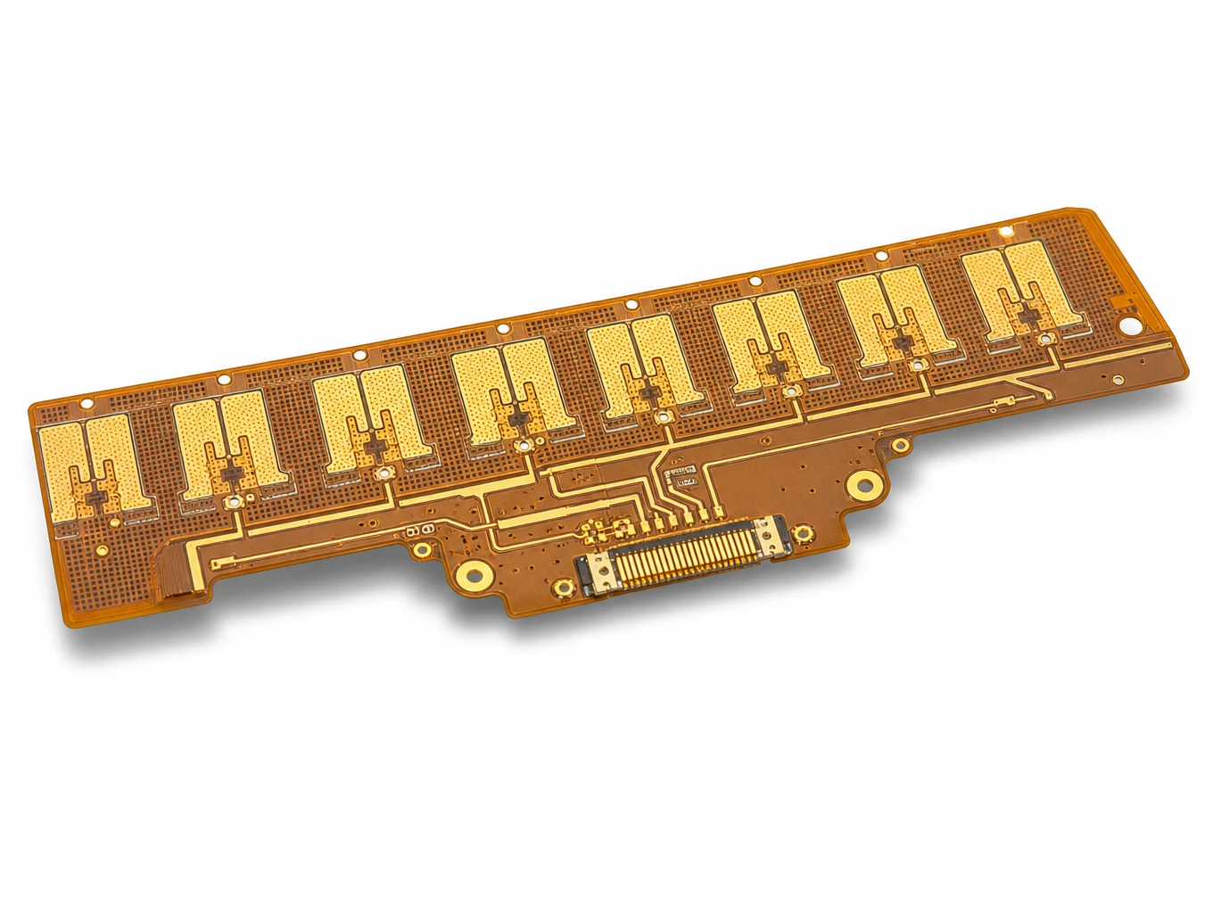
5G mmWave Antenna Array & RF Front-End LCP FPC
Model: TLX-COMM-5G01
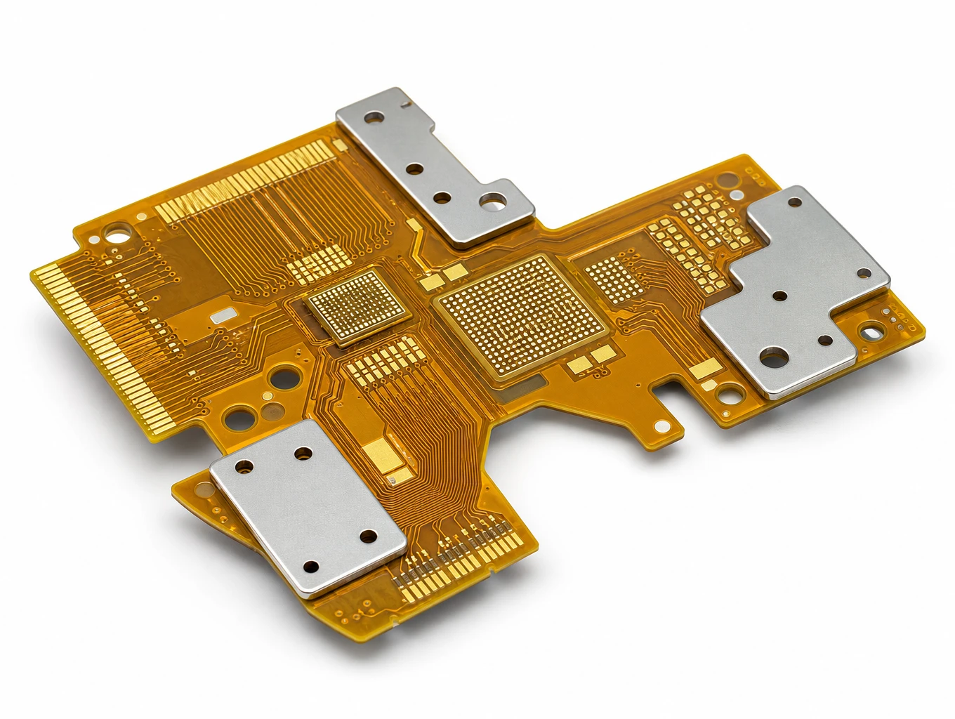
400G/800G High-Speed Optical Transceiver Multi-Layer Flex PCB
Model: TLX-COMM-OPT03
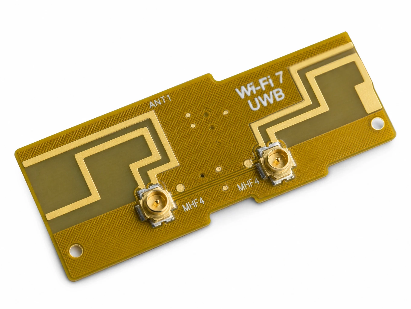
Wi-Fi 7 & Ultra-Wideband (UWB) Spatial Positioning Antenna FPC
Model: TLX-COMM-UWB06
Related FPC Solutions
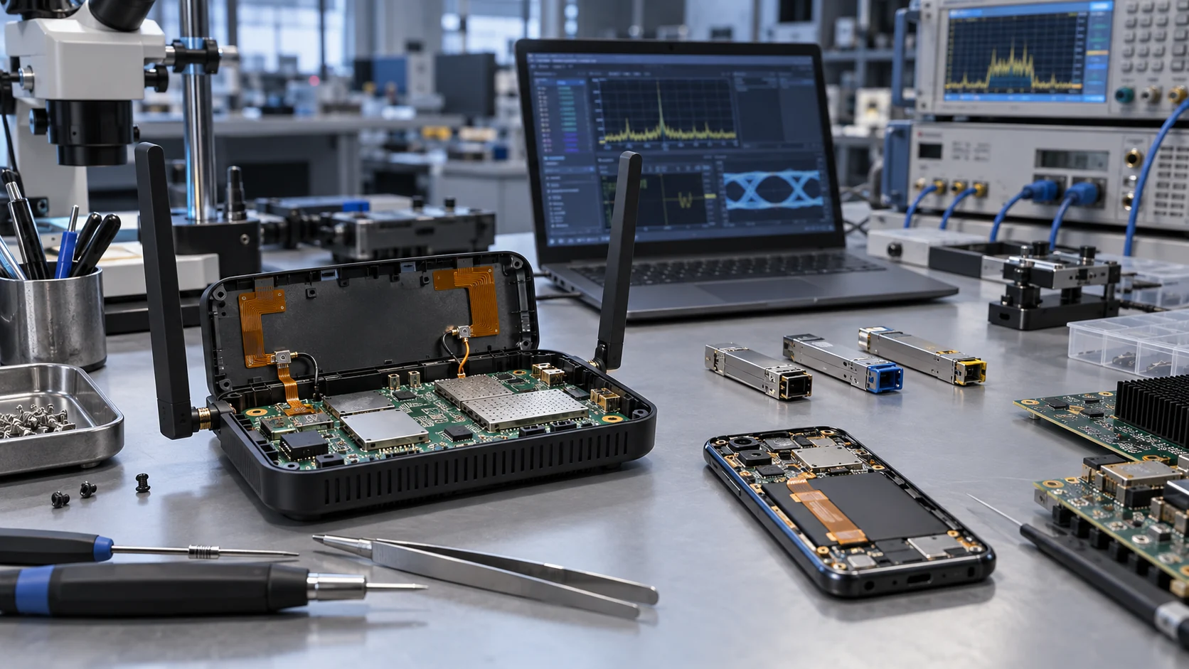
RF & Communication FPC Solutions
Custom RF flexible PCB and telecom interconnects for antenna modules, wireless terminals and high-speed communication assemblies. Coordinate materials, signal paths, shielding and connector support with Teleconix before prototype release.
Explore Solutions
Consumer Electronics & Smart Card FPC Solutions
Custom flexible circuits for smart cards, TWS earbuds and compact wearables. Align routing, stack-up, component interfaces and prototype acceptance with Teleconix before releasing your OEM design.
Explore Solutions
Display FPC
Display FPC products for OLED, AMOLED, micro-LED and TFT-LCD modules in handheld, wearable, automotive and industrial devices. Review the display interface, connector and installed flex shape together.
Explore Solutions RF & Communication FPC Solutions
Custom RF flexible PCB and telecom interconnects for antenna modules, wireless terminals and high-speed communication assemblies. Coordinate materials, signal paths, shielding and connector support with Teleconix before prototype release.
Explore Solutions Consumer Electronics & Smart Card FPC Solutions
Custom flexible circuits for smart cards, TWS earbuds and compact wearables. Align routing, stack-up, component interfaces and prototype acceptance with Teleconix before releasing your OEM design.
Explore Solutions Display FPC
Display FPC products for OLED, AMOLED, micro-LED and TFT-LCD modules in handheld, wearable, automotive and industrial devices. Review the display interface, connector and installed flex shape together.
Explore SolutionsFrequently Asked Questions
Conclusion: connect the telecom design to release evidence
A useful telecom flexible PCB specification connects the intended signal path to the installed assembly and its release evidence. Define RF feeds, digital channels and antenna elements separately, then coordinate materials, connectors, supports and test ownership across the complete product.
Prepare the controlled interface matrix and sample plan before requesting a production proposal. Discuss your telecom FPC project with Teleconix and share the intended application, drawings and acceptance requirements for a focused review.