
Flex PCB coverlay: define protection and access together
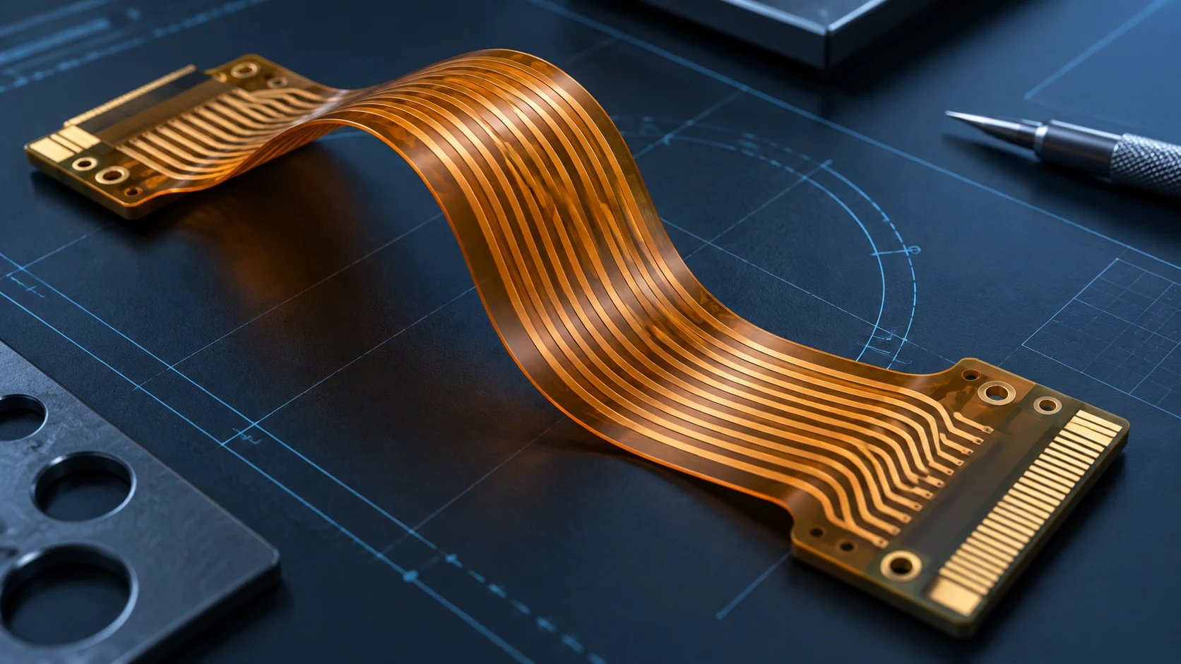
Flex PCB coverlay is a protective insulating layer over the copper circuitry of a flexible board, with openings where contacts, solder joints or test access are needed. A conventional construction uses polyimide film and a bonding adhesive. The released design must describe both the areas to protect and the finished areas that must remain exposed.
For an OEM, the important deliverable is a usable interface. A component pad must remain accessible after fabrication. A connector tail must match its mating drawing. A moving section needs a construction selected for its actual route and motion. Those requirements should be reviewed together before the opening artwork is approved.
This guide focuses on coverlay selection, opening definition and inspection. Start with the flexible PCB materials guide for the wider copper and dielectric choices. The practical checklists below help engineering, purchasing and quality teams turn an initial layout into an agreed fabrication package.
Compare film coverlay and flexible solder mask by region
Film coverlay and photoimageable flexible solder mask use different manufacturing processes. A fabricator may propose film over a bending region and a qualified flexible coating around dense component features. The decision needs to account for opening geometry, assembly access and the mechanical duty of each region.
Würth Elektronik lists separate pad-clearance and bridge-width rules for coverlay and photosensitive flex solder mask in its PURE.flex documentation. This is a useful reminder that one set of rigid-board mask rules should not be copied into every flex design. The published figures apply to that supplier’s construction and are not Teleconix capability specifications.
Ask the proposed manufacturer to identify the material and process for each region. Do not assume every solder mask formulation is suitable for flexing, or that a film construction automatically qualifies the finished circuit for repeated motion.
| Review item | Film coverlay | Flexible solder mask |
|---|---|---|
| Construction | Film and bonding system | Specified coating system |
| Opening review | Cutting, registration and adhesive effects | Imaging and coating process limits |
| Release evidence | Finished access and coverage checks | Feature definition and application suitability |
Specify the film and adhesive as one material system
A drawing that states only “polyimide coverlay” leaves important decisions unresolved. Identify the film thickness, adhesive system and nominal adhesive thickness, or request a documented supplier proposal. State whether equivalents are permitted and who approves a substitution. Keep the approved material reference with the stack-up revision.
Ask how the proposed bonding system suits the actual copper construction and assembly exposure. The useful answer connects the chosen materials with fabrication and verification. A generic material name, colour or maximum temperature from a marketing page does not define the completed circuit’s performance.
For quotation comparison, list the assumptions beside the price. If one supplier changes film thickness or adhesive, engineering should review the effect on the overall construction before purchasing accepts the alternative. Ask for material documentation appropriate to the project without implying that a specific brand or certification is already required.
Record requirements at the level that the supplier can verify: material identification, agreed thickness information, coverage and any project-specific environmental checks.
Define the finished pad exposure before the artwork allowance
Begin with the functional requirement at the copper feature. Show which part of a pad must remain available for soldering, probing or connector contact. Then agree the opening artwork with the fabricator. Keep the required finished exposure distinct from an artwork expansion entered in CAD.
Registration variation, the opening process and adhesive behaviour all belong in that discussion. Epec’s manufacturing guidance identifies these as relevant considerations for laminated coverlay. A smaller nominal opening may look tidy in a viewer while leaving too little accessible pad on the completed part.
Ask for a marked review drawing showing the intended opening boundary, copper boundary and critical measurement locations. For a sensitive feature, identify the minimum acceptable exposed area and the adjacent conductor that must stay protected. This gives the supplier a functional target instead of a vague instruction to “increase the opening.”
Do not assign a universal clearance from an unrelated example. The approved number should come from the proposed construction, process and geometry, with any fabrication compensation documented.
Review individual openings and shared windows
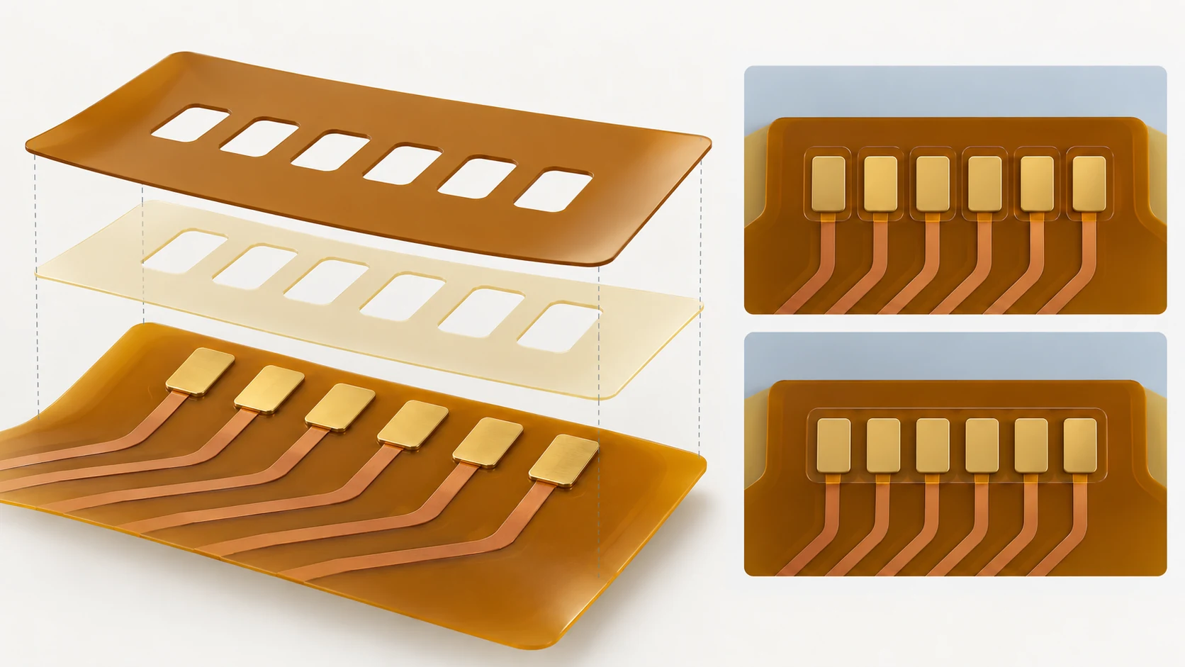
An individual opening can isolate access to one pad. A shared window exposes a group of pads. Where pads are close together, ask whether the remaining film bridges are practical for the proposed process. Compare alternatives with the assembler before approving a change that exposes additional copper.
A shared window may simplify the coverlay geometry, but the assembly team still needs a suitable solder-paste and placement plan. Identify nearby traces, test features and unused pads that become exposed. Confirm what surface treatment is required on those areas and whether handling creates an additional concern.
Use a local enlarged drawing to compare the alternatives. Label the pad pitch, copper dimensions, opening outline and surrounding coverage. Ask the fabricator to state which features drive its recommendation and whether the proposed change affects tooling or lead time.
Select the arrangement that meets the electrical and assembly requirements with an agreed manufacturing process. Treat the choice as a local design decision rather than a rule that every fine-pitch component needs the same opening pattern.
Check connector tails and stiffener boundaries together
At a connector tail, the contact pattern, exposed length, insertion direction and finished thickness must match the actual connector documentation. Show where coverlay ends relative to the contact fingers and reinforcement. Review the full mating region rather than considering its protective film separately.
The flexible PCB stiffener guide explains how local reinforcement contributes to connector fit. Use the same reference features for the coverlay boundary and the support outline so that the two drawings can be compared directly. Identify which layers are present at each finished-thickness measurement point.
During prototype assembly, check insertion and latch operation with representative parts. Record whether the exposed contacts seat correctly and whether the coverlay boundary interferes with the intended route. If an adjustment is required, update both the circuit and mechanical documents.
A successful electrical continuity result does not verify connector fit. Keep dimensional, installation and electrical observations as separate entries in the acceptance record.
Keep openings consistent with the intended bending route
Show the installed bend envelope alongside the coverlay layout. Locate component pads, test access and connector regions in that mechanical context. A flat artwork review alone cannot reveal whether an exposed area or a material boundary lands at a forced crease after the housing closes.
Use the flex PCB bend radius guide to describe installation bends and repeated movement. Provide the actual route, available clearance and support locations. Ask the manufacturer to review the proposed protection system for that duty rather than inferring suitability from the word “flexible.”
If a prototype requires extra folding to reach its connector, record the assembly sequence and determine whether that handling is intended. Do not validate only the final resting position while ignoring the movement required during installation or service.
Any motion test should identify the sample construction, fixture, travel, environment and acceptance criterion. A coverlay material selection alone is not a quantified fatigue-life result.
Include coverlay in the electrical construction review
For a sensitive signal path, give the electrical reviewer the actual regional stack-up, including protective materials above the conductors. Identify where that construction changes and where openings interrupt it. The model should represent the proposed finished circuit rather than an earlier copper-only sketch.
The controlled impedance flex PCB guide helps organize signal targets, return paths and verification. Here, the practical task is to keep the coverlay definition synchronized with the electrical model. A substitution or a local opening change should be visible to whoever owns that review.
Ask which material properties and thickness assumptions the model uses. If a supplier proposes a different protection system, record whether the electrical review needs to be repeated. Do not treat a continuity test as evidence that a controlled-impedance requirement has been met.
This coordination is particularly useful when a layout combines connector contacts, dense components and longer protected routing within one small assembly.
Separate coverlay outputs from solder-paste data
The fabrication package should identify the coverlay outline and openings for each side. Solder-paste apertures describe a different operation and should have unambiguous names. Add a layer map that allows a reviewer to distinguish copper, protection, paste, outline and reinforcement without guessing from file extensions.
Altium’s coverlay documentation explains that custom coverlay and solder mask can appear together in a display while being exported separately. It also distinguishes pad openings from polygonal outlines and cutouts. Whatever CAD system you use, inspect the manufacturing outputs in a viewer before release.
Use the flexible PCB design checklist for the wider handoff. Compare the top and bottom sides, layer polarity, origin and revision. Confirm that the receiver interprets a shape as an opening or retained material exactly as intended.
Archive the approved output package with the review response. An emailed screenshot is useful context, but it should not silently replace the controlled fabrication files.
Coordinate soldering, inspection and rework access
Ask the assembler to review exposed pad area, nearby coverlay steps and access for inspection. Include the intended component and connector part numbers. A layout that appears acceptable as a bare circuit may create a difficult assembly or inspection condition after parts are placed.
The FPC assembly guide covers fixtures and process responsibilities. For coverlay, add a local review of paste printing, component seating and any features that need probing. Discuss whether a shared window changes the assembly plan before treating it as a simple fabrication correction.
Define permitted rework and the evidence needed afterward. If a part needs a second thermal cycle or local repair, the responsible teams should assess the actual material system and process. Avoid creating a generic rework-temperature rule without the component, material and assembly requirements.
Include packaging and handling instructions where exposed contacts or unsupported areas need protection. Make those instructions part of the agreed delivery scope.
Use a prototype checklist with observable acceptance criteria
A useful coverlay inspection record connects a feature to a requirement and a measurement. Check identification and revision first. Inspect coverage, accessible pad area, visible edge condition and the critical boundaries named in the drawing. Define sampling and magnification with the supplier rather than relying on “good appearance.”
Combine those observations with the flexible PCB prototype validation plan. Check the circuit in its intended connector, fixture and enclosure. Keep observations from bare-board inspection separate from the results after assembly so the team can identify where a discrepancy appears.
- Confirm top and bottom coverlay match the released revision.
- Measure critical finished openings and connector exposure.
- Inspect designated edges and areas for agreed bond acceptance.
- Check assembly access and the installed route.
- Record sample identity, method, result and disposition.
If a feature fails, preserve photographs and measurements before modifying the sample. Compare the finding with the approved drawing and supplier exceptions. This helps distinguish a manufacturing discrepancy from a requirement that was never specified clearly.
Work through a handheld-device review example
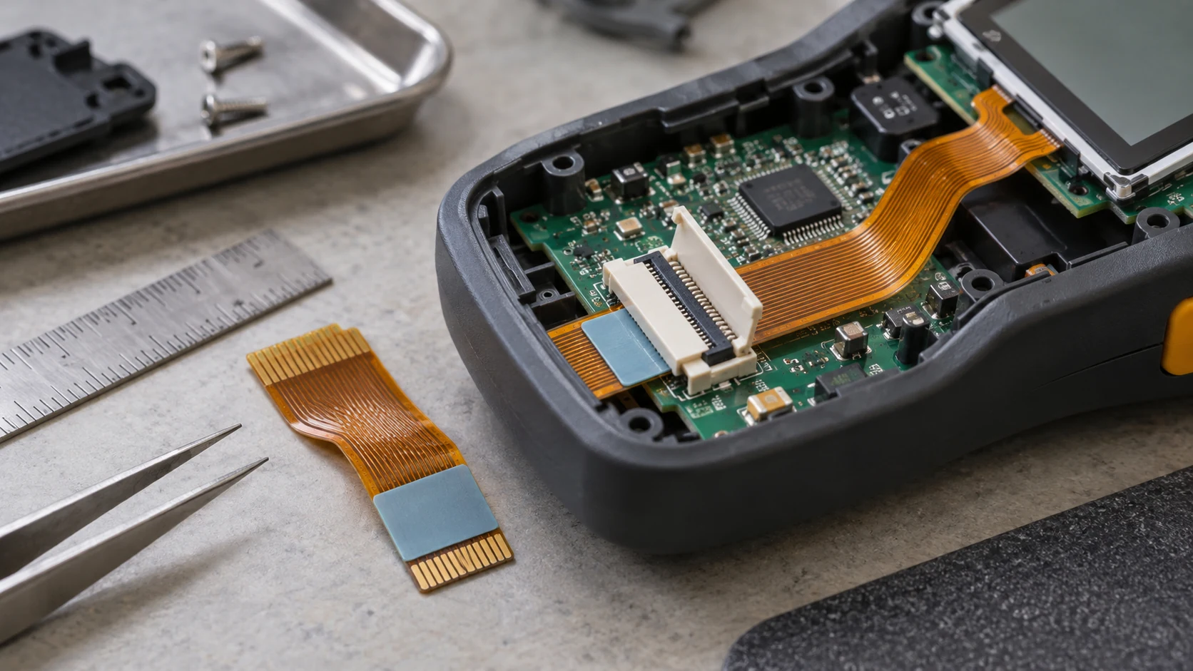
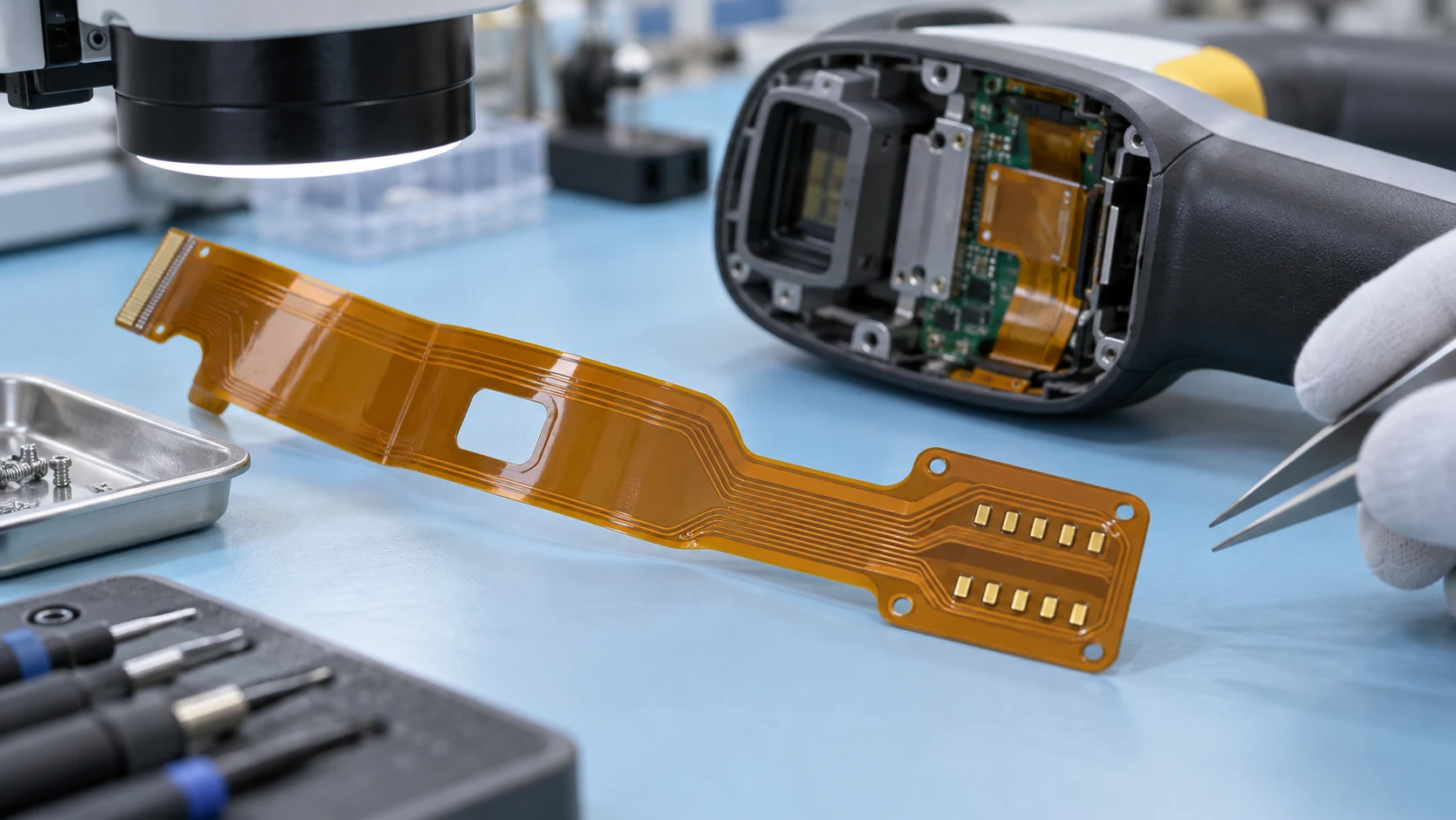
Consider an illustrative handheld scanner with a flex tail connecting a display to its main board. The tail includes contact fingers, an assembled component area and a protected section routed around an internal support. These are three different review locations even though they share one circuit outline.
At the fingers, the team checks exposed contact length and finished mating thickness against the connector drawing. At the component area, the assembler compares individual openings with a shared window and identifies any newly exposed traces. Along the installed route, the mechanical reviewer checks that the housing does not force a fold at an opening or support boundary.
The supplier returns a marked drawing identifying the proposed material system and any changes. Engineering approves the geometry, purchasing references the new revision, and the prototype checklist records fit, pad access and the assembled route separately. This example is a review method, not a report of a completed Teleconix customer project. It shows how to close specific questions without treating one successful inspection as proof of every requirement.
Prepare a coverlay RFQ that supports fair comparison
Send the proposed stack-up, protection-layer files, assembly data and application conditions together. Identify unresolved choices explicitly. A supplier can then quote the defined build or return a documented alternative, instead of silently making assumptions about pad exposure or material selection.
Ask the quotation to separate samples, production quantities, tooling and optional verification. Request a list of technical exceptions and the revision used for pricing. If an alternative needs a new opening layout, include the engineering review and prototype consequences when comparing totals.
Use the flexible PCB cost guide to structure the broader comparison and the FPC manufacturing guide to define relevant quality records. Avoid buying an apparently cheaper quotation that omits an inspection or assembly requirement needed by the project.
Before ordering, close the material proposal, drawing changes and acceptance plan. Keep the approved response with the purchase documentation so the first lot is judged against the same requirements used during quotation.
Control substitutions and keep the supporting references
A change to the film, adhesive, thickness, opening process or geometry should trigger a review of the affected requirements. List the possible impact on pad access, connector fit, assembly exposure and electrical construction. Decide which checks must be repeated and record the approved revision.
Use supplier documentation to resolve specific technical questions. Published design rules are useful references, but they do not establish that a different manufacturer uses the same process. Confirm Teleconix’s proposed manufacturing and inspection scope for the actual design before releasing an order.
Technical references
See Würth Elektronik PURE.flex design rules for process-specific geometry examples, Epec’s coverlay and soldermask manufacturing discussion for fabrication considerations, and Altium’s coverlay output documentation for CAD handoff details.
Related Products
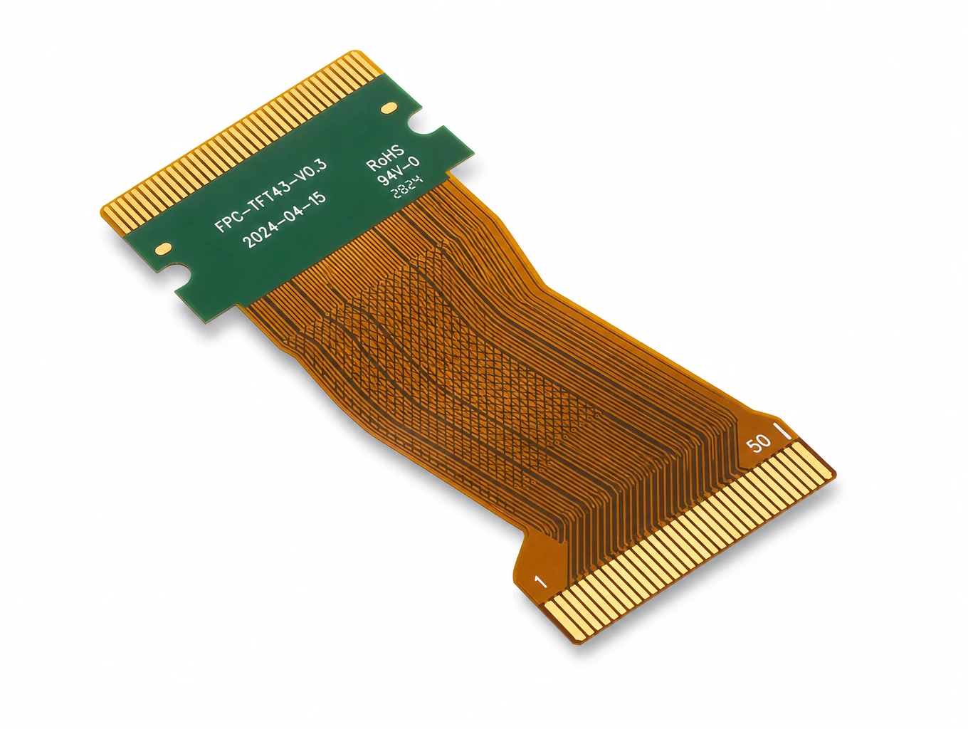
Industrial HMI & TFT-LCD Module FPC
Model: TLX-DFPC-IND05
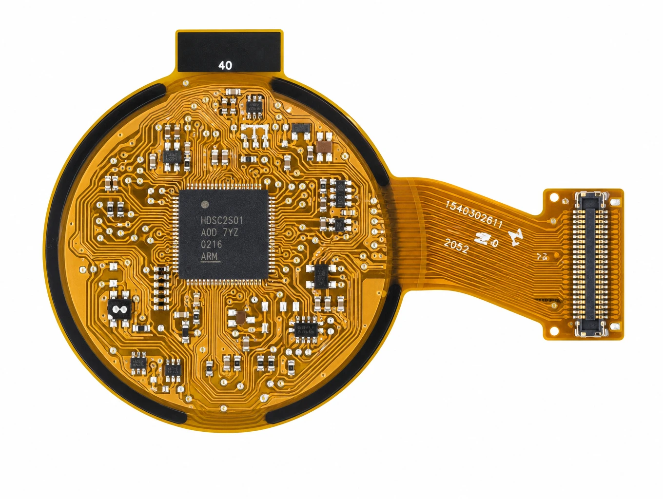
Wearable Smartwatch & Round AMOLED FPC
Model: TLX-DFPC-WEAR04
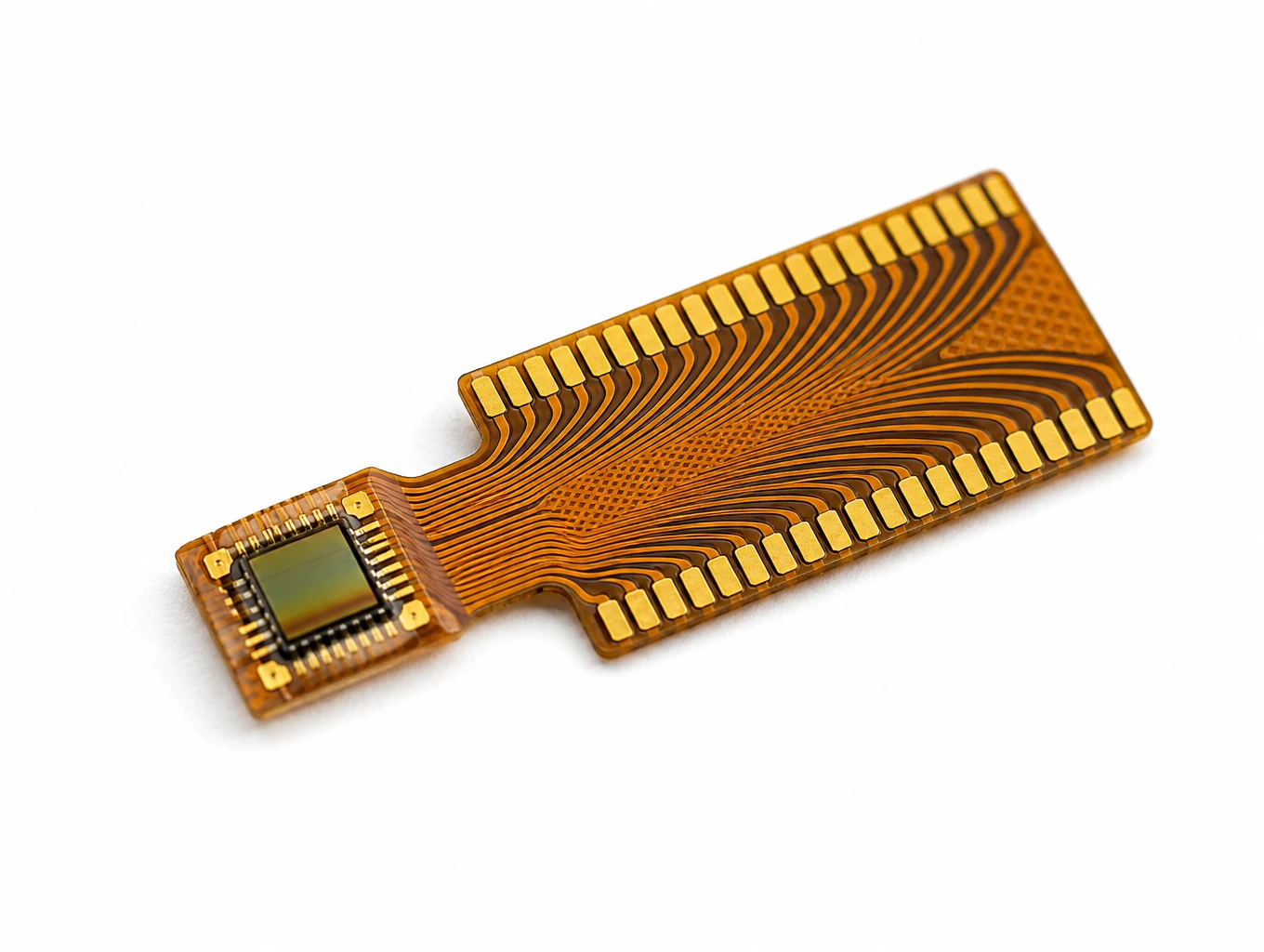
Medical Endoscope Micro-Display FPC
Model: TLX-DFPC-MED06
Related Solutions

Display FPC
Teleconix manufactures fine-pitch, high-density FPCs for LCD, OLED, mini-LED displays, camera modules, and optical sensors — delivering stable signal transmission and exceptional brightness control.
Explore Solutions
Medical Device FPC Solutions
Custom flexible circuits for diagnostic equipment, patient monitoring and compact medical electronics. Discuss routing, signal paths, materials and prototype acceptance with Teleconix before releasing your OEM design.
Explore Solutions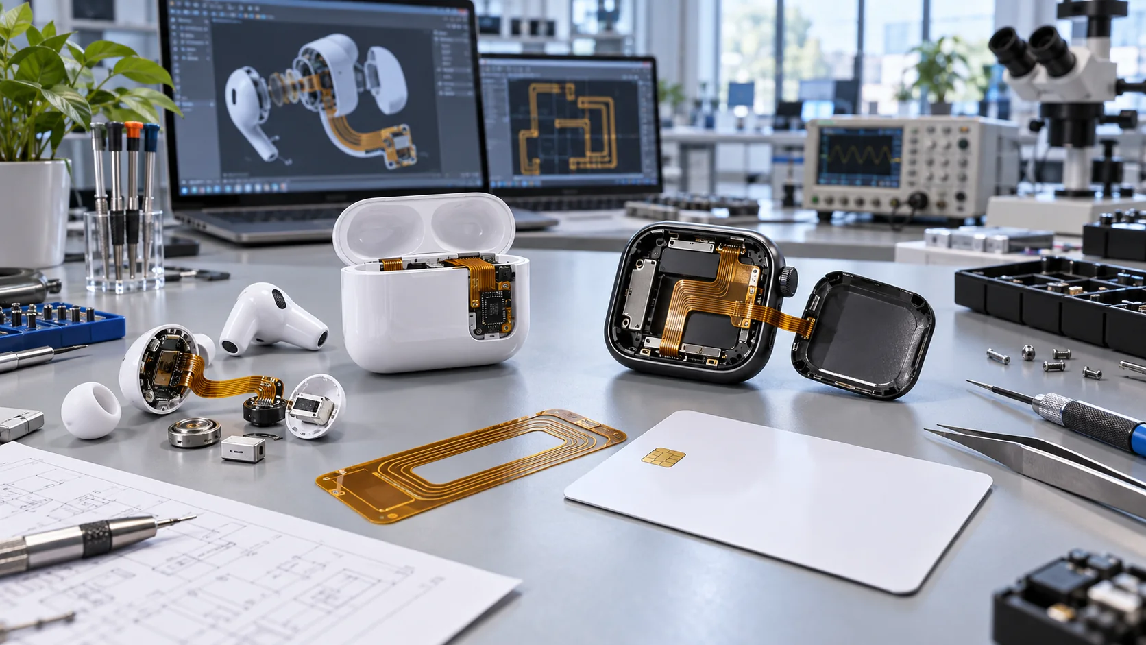
Consumer Electronics & Smart Card FPC Solutions
Custom flexible circuits for smart cards, TWS earbuds and compact wearables. Align routing, stack-up, component interfaces and prototype acceptance with Teleconix before releasing your OEM design.
Explore Solutions Display FPC
Teleconix manufactures fine-pitch, high-density FPCs for LCD, OLED, mini-LED displays, camera modules, and optical sensors — delivering stable signal transmission and exceptional brightness control.
Explore Solutions Medical Device FPC Solutions
Custom flexible circuits for diagnostic equipment, patient monitoring and compact medical electronics. Discuss routing, signal paths, materials and prototype acceptance with Teleconix before releasing your OEM design.
Explore Solutions Consumer Electronics & Smart Card FPC Solutions
Custom flexible circuits for smart cards, TWS earbuds and compact wearables. Align routing, stack-up, component interfaces and prototype acceptance with Teleconix before releasing your OEM design.
Explore SolutionsFrequently Asked Questions
Conclusion: release coverlay requirements with the circuit
Successful flex PCB coverlay design connects material selection with finished pad access, mechanical routing and assembly verification. Define the functional requirement first, agree the manufacturing allowance and retain a clear inspection record. Keep changes synchronized across the stack-up, artwork and order package.
Bring your proposed files and application requirements to Teleconix for a coverlay and FPC project discussion. The OEM and ODM project page can help organize the wider request. Confirm the proposed construction, delivery scope and acceptance plan before production release.