
Multilayer flexible PCB: start with the required interconnect
A multilayer flexible PCB uses more than two conductive layers separated by insulating materials in a flexible circuit construction. Additional layers can create routing space and support defined reference paths, but they also change thickness, manufacturing steps and mechanical behaviour. Start with the connection problem and approve the construction before treating the layer count as a finished specification.
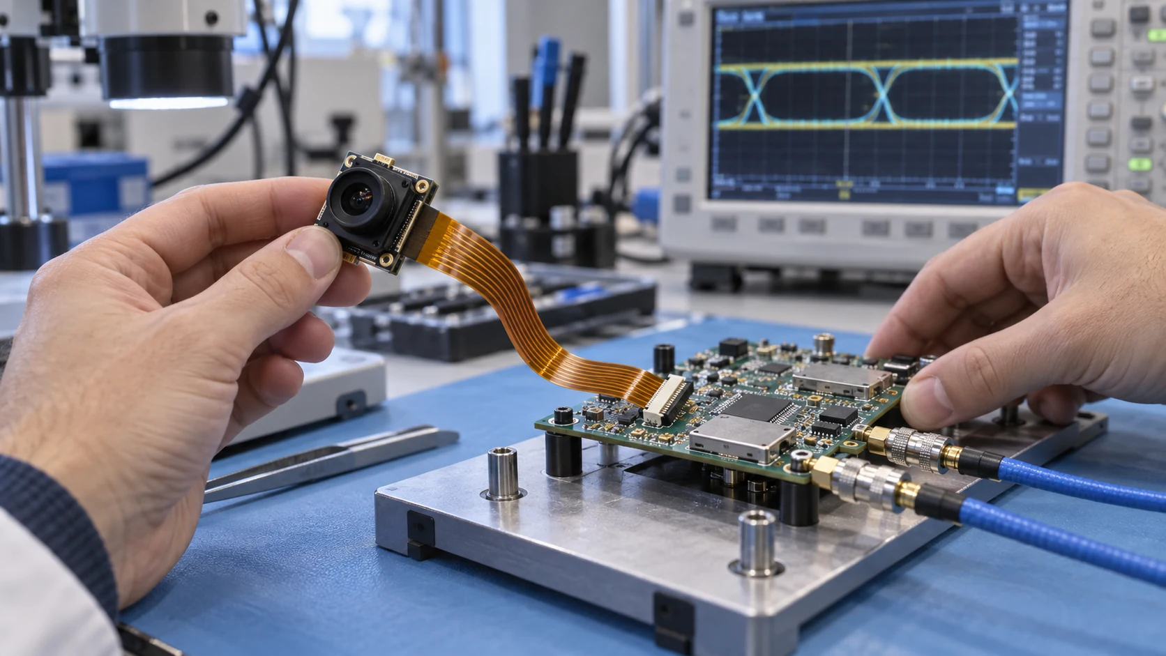
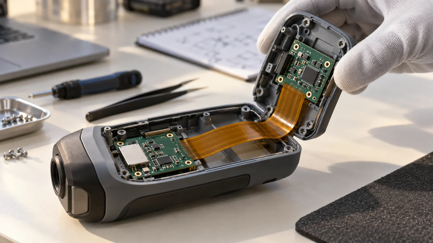
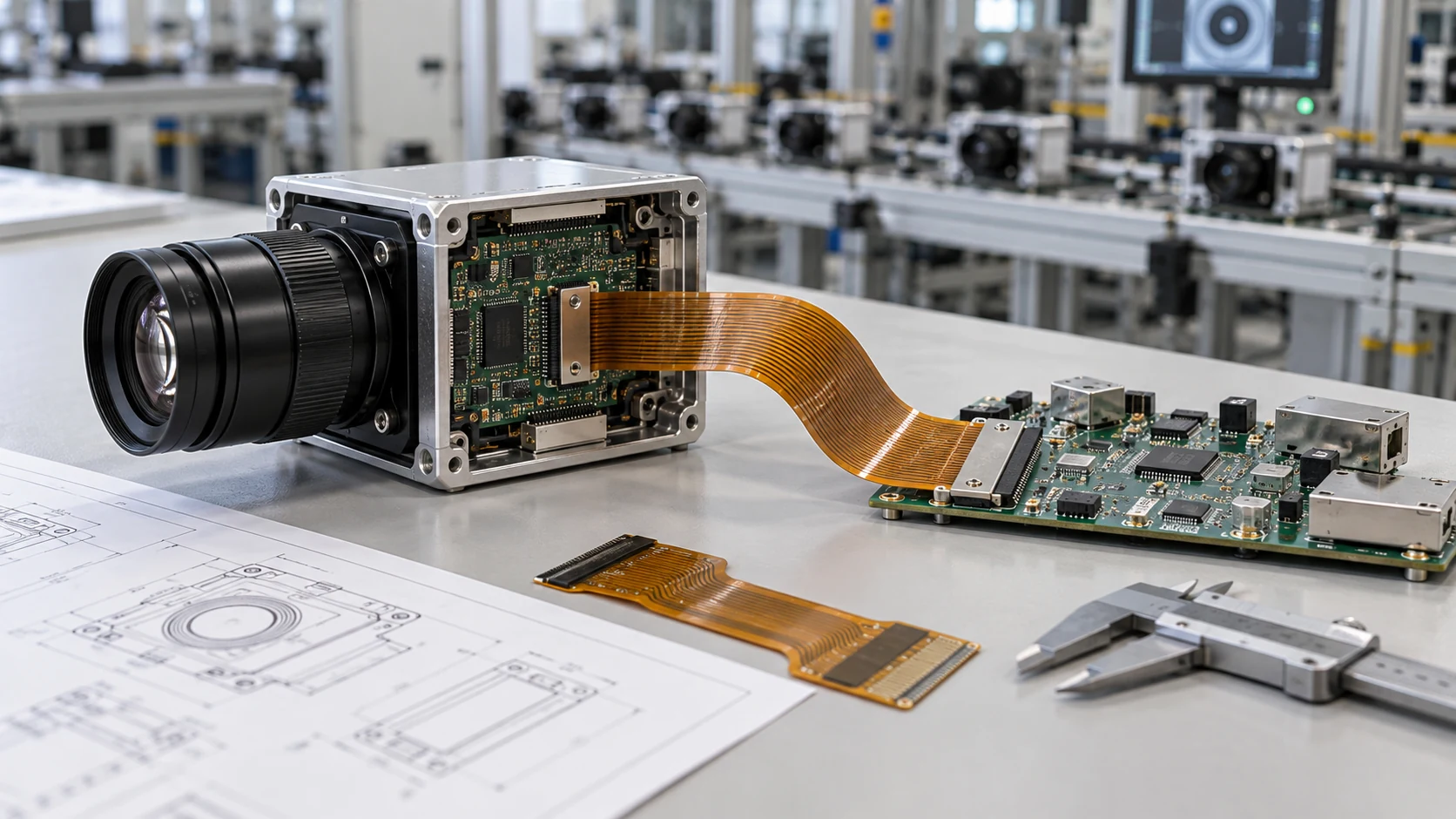
For an OEM team, the useful question is whether the proposed circuit will fit, carry the intended signals and survive the actual installation or movement. A compact camera head, communication module or industrial instrument may need dense connections without a bulky cable harness. Each application still needs its own layout, material system and verification plan.
This guide explains how to turn those needs into a controlled stack-up, fabrication package and quotation review. Use the flexible PCB design checklist for the wider design release process. The following decisions help engineering, quality and purchasing agree what a supplier is being asked to build.
Decide whether extra copper layers solve a real problem
Write down the constraints that justify additional routing layers. These may include the number of nets, connector pitch, separation of sensitive signals, the available outline and the need for a continuous reference path. Distinguish a routing limitation from an inconvenient component placement. Moving a connector or changing the system partition can sometimes avoid a more complicated circuit.
Ask the designer to compare a simpler construction with the proposed multilayer version using the same enclosure and electrical requirements. Record what each option changes in width, thickness, interfaces and assembly. Do not assume the smaller bare circuit produces the smaller finished assembly; connector bodies, support features and service access also occupy space.
- Identify the specific nets or interfaces that need another layer.
- Explain where a reference conductor must remain continuous.
- Check whether the proposed outline can be handled and assembled.
- Compare the complete interconnect cost and qualification effort.
The outcome should be a short design rationale that purchasing can include with the RFQ. It gives suppliers a reason to explain an alternative rather than simply quoting the requested layer count.
Separate multilayer flex, local stiffeners and rigid-flex
A multilayer flex circuit and a rigid-flex PCB can share materials and fabrication operations, but the names describe different structures. In a multilayer flex design, the conductive stack belongs to the flexible construction. A local stiffener provides mechanical support. A rigid-flex design incorporates rigid circuit regions that can contain their own routed copper layers.
This distinction matters at connector tails and component islands. A reinforcement plate under the flex does not automatically turn the assembly into a routed rigid-flex board. Review the flexible PCB stiffener guide when the requirement is local support, and the rigid-flex design and sourcing guide when rigid circuit regions form part of the electrical structure.
Label the intended construction clearly on the drawing. Identify which materials carry circuitry, which support the assembly and which are temporary manufacturing tooling. Ambiguous terms can lead two suppliers to propose different products under the same quotation description. A simple section sketch and a region map are usually more useful than a long list of interchangeable product names.
Approve the multilayer flex PCB stack-up before detailed routing
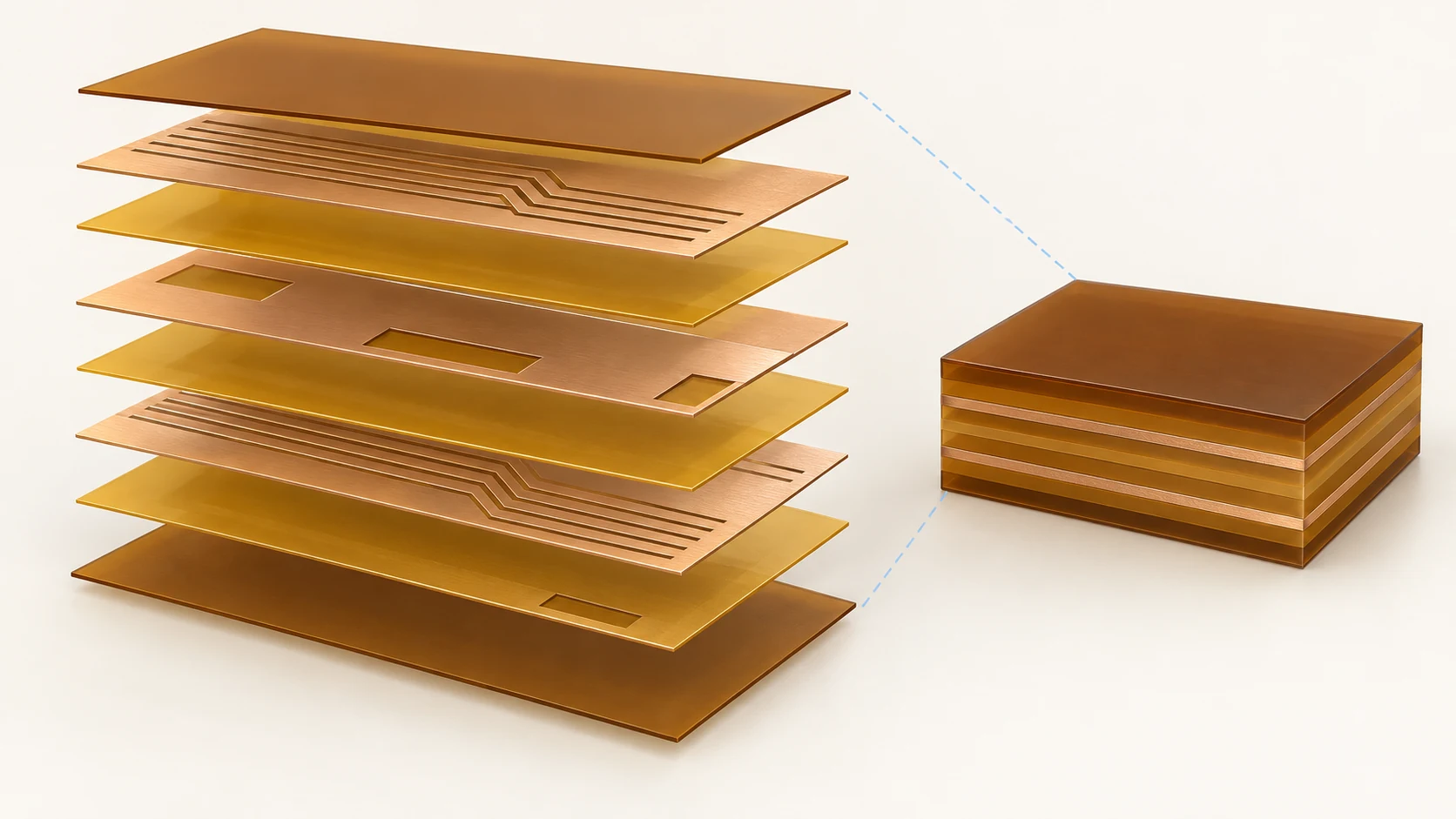
A multilayer flex PCB stack-up should show the conductive layers in order, their intended functions and the dielectric or bonding materials between them. Include external protection, local reinforcement and any region where the construction changes. The complete thickness matters at a connector, a mounting feature and a bend, even when the copper itself is thin.
Assign each layer a design purpose. A signal layer without a suitable reference path may not achieve the expected electrical result. A reference layer added everywhere may create unnecessary mechanical or processing constraints. Review the electrical and mechanical requirements together, then ask the manufacturer to propose a buildable material arrangement.
Altium describes the different roles of flexible materials, mechanical stiffeners and routed rigid regions in its layer-stack construction overview. Use the distinction to clarify drawings; confirm the actual materials and regional stack-up with the selected fabricator.
Freeze the layer order and naming convention before output generation. The fabrication drawing, CAD layers, impedance notes and assembly views should use the same revision and the same names.
Select materials as a complete process-compatible system
Polyimide, copper foil, bonding layers and surface protection work together in the finished part. Compare proposed material systems by the required electrical behaviour, installed thickness, mechanical duty and assembly exposure. A familiar film name alone does not establish that an entire multilayer construction is suitable.
Use the flexible PCB materials selection guide to prepare the wider material discussion. For this RFQ, request the proposed layer materials, copper construction and bonding process, including any substitution the manufacturer wants to make. Explain whether the substitution changes thickness, electrical models or the agreed qualification evidence.
Include storage and handling in the conversation with fabrication and assembly suppliers. Moisture control and thermal processing depend on the actual material system, packaging and assembly sequence. Ask for documented instructions that match the delivered parts instead of copying a generic baking schedule from another product.
Approve substitutions through a named engineering owner. Record the original material, proposed replacement, reason for the change and required checks. The approved alternative then belongs in the released drawing and purchase specification, not only in an email attached to a quotation.
Define installation bends and repeated motion separately
Describe how the circuit is used after delivery. A circuit formed once inside a sealed enclosure has a different duty from one that moves during every operating cycle. Service opening and repeated connector handling can add movement even when the normal operating route remains fixed.
Provide the intended three-dimensional route, bend direction, available clearance and mechanical restraints. Use the static and dynamic bend-radius guide to organise those inputs. Do not select a bend radius from layer count alone; the construction, copper distribution and actual movement conditions require review.
For moving equipment, record stroke or angle, cycle expectations, motion speed, environmental conditions and the places where the circuit is restrained. Ask whether a thinner dedicated moving section or a different interconnect architecture is appropriate. A circuit that can be folded for installation should not automatically be specified for continuous dynamic use.
Keep mechanical acceptance observable. Identify the installed geometry to inspect and the operating movement to reproduce in the prototype fixture. A photograph of a flat sample cannot confirm that the final routed assembly meets those conditions.
Place vias and layer transitions in reviewed regions
Layer changes need a documented interconnection strategy. Through holes, blind vias and buried structures are different fabrication choices. Define the intended connections and ask the supplier to confirm which processes are available for the proposed construction. More layers do not automatically mean that every via arrangement is practical.
Locate vias and component joints away from regions intended to bend, and review transitions where the construction or stiffness changes. Würth Elektronik identifies bending-area via restrictions in its SLIM.flex design rules. Those rules describe its specific technology; they are not universal capability values for another manufacturer.
For the quotation, supply the drill and interconnection data, identify critical layer pairs and distinguish the required finished hole from the fabrication tool size. Request written feedback on unsupported structures, registration assumptions and any changes to capture pads or clearances.
Keep the agreed changes visible in the released CAD and drawing. If a supplier proposes a different via sequence, review its impact on routing, inspection, processing and reliability evidence before accepting the quotation.
Review reference paths and impedance across the complete channel
Additional copper layers can support useful signal-reference arrangements, but an added plane does not by itself establish signal integrity. Identify which layer each critical signal uses, its reference conductor and the transitions between connector, flex and adjoining boards.
For an impedance-controlled interface, provide the target, tolerance and measurement agreement with the proposed stack-up. The supplier needs the relevant geometry and material assumptions. Use the controlled-impedance flex PCB planning guide to distinguish a fabrication coupon measurement from complete channel performance.
Discuss openings, copper pattern changes and shielding features where they affect the reference path. A mechanical modification can change the electrical model. Avoid approving an enclosure fit change without asking the electrical designer whether the model or validation needs updating.
Plan a system-level check for the actual interface when its performance requires one. A bare-board continuity test, an impedance coupon and a functional communication test answer different questions. Define who performs each check, which revision is tested and what evidence is delivered with prototype approval.
Coordinate coverlay, contacts and connector-tail thickness
External protection and exposed contacts are part of the stack-up review. Define where conductors remain covered and where pads, contact fingers or test points must be accessible. A dense component area may need a different protection approach from a section that is formed during installation.
Use the flex PCB coverlay opening guide to describe finished exposure and opening artwork. Ask the fabricator and assembler to review the access required for soldering, inspection and rework. An opening that is easy to draw may still conflict with the actual process or nearby copper.
At a connector tail, check the finished thickness of every material that enters the mating interface. Include copper, dielectric, protection, reinforcement and bonding layers where applicable. Use the connector manufacturer’s drawing to identify the contact side, insertion direction, permitted thickness and retained length.
State critical finished dimensions separately from nominal layer values. Then explain the inspection datum and method. This helps the supplier evaluate the complete interface instead of independently accepting several nominal dimensions that may not produce an acceptable finished tail.
Prepare support, panel handling and assembly access
A multilayer construction still needs a practical assembly plan. Define the handling panel, component support and the way the circuit will be released into the final outline. Review access for placement, soldering, cleaning, inspection and connectors before locking the layout.
For populated parts, include the BOM, placement data and assembly drawings with the fabrication files. Use the FPC assembly and quality-control guide to separate permanent reinforcement from temporary support tooling. Explain which supports remain in the finished device and which are removed during production.
Check whether the assembler can handle the proposed part after depanelisation. Long unsupported branches, small islands and projecting contacts may need a different handling sequence. Manufacturing convenience should be evaluated alongside the enclosure fit and required electrical interface.
Assign ownership for the assembly assumptions. A bare-board quotation may exclude tooling, components, connector installation or functional testing. If another supplier performs assembly, agree the handover condition, packaging and acceptance checks between the two operations.
Release one consistent fabrication and RFQ package
The RFQ should let a supplier reconstruct the intended product without choosing between conflicting documents. Provide one revision identifier and a simple list of the files that belong to it. Identify reference information separately from released manufacturing data.
- Layer order, proposed materials and region-specific thickness requirements.
- Circuit artwork, outline, drill data and required interconnections.
- Flat and installed mechanical views with named bend and support regions.
- Coverlay or protection openings, contact finish and connector drawings.
- Assembly data, quantities, project stage and expected delivery condition.
- Critical dimensions, electrical requirements and agreed acceptance records.
Ask for a written assumptions and exceptions list. A supplier should identify what it has interpreted, changed or excluded. Respond to those points through engineering review and update the package where necessary. A clean quotation comparison starts with a clean product definition.
Altium’s flex-region design documentation illustrates why board regions and stack assignments must agree. Whatever CAD tool is used, inspect the exported data and drawing together before release.
Compare quotations using the same approved construction
Price comparisons are useful only when the suppliers are quoting equivalent scope. Compare materials, layer construction, interconnections, support features, finish, testing and the delivered condition. Ask whether prototype processing is representative of the planned production route.
Use the flexible PCB cost-driver guide to organise one-time tooling and recurring production costs. Additional layers can affect processing, inspection and yield assumptions, but a universal cost multiplier is not a reliable basis for an OEM purchasing decision.
Record supplier exceptions next to the affected requirement. Examples include an alternate material, a different opening process or a test excluded from the base price. Ask the technical owner to approve those differences before purchasing treats two figures as directly comparable.
For a proposed four-layer flexible PCB, label it as a candidate construction until the manufacturer has confirmed the build. Layer count is a design input, not evidence of a supplier’s capability. Include the actual quantities and required milestones so quotation discussions focus on the project being procured.
Validate the prototype in its installed configuration
Plan prototype acceptance before placing the order. Check the received revision, delivered construction and critical dimensions, then evaluate the circuit in the intended enclosure or a representative fixture. Keep the flat inspection results and installed test results tied to the same sample identifiers.
Use the flexible PCB prototype validation guide to define mechanical fit, electrical checks and project sign-off. Include connector mating, assembly support, bend routing and the complete functional interface where relevant. A successful bare-board test does not replace these assembly checks.
When reliability testing is needed, agree the construction, sample conditions, loading, environment and failure criteria with the responsible engineering team. Record deviations and the decision made from them. Do not transfer a test result from a different material system or mechanical route without a reasoned comparison.
Keep a clear approval record: what was tested, which requirement it addressed, who reviewed the evidence and which issues remain open. That record gives purchasing a defensible basis for moving from prototype samples to the next production stage.
Control DFM changes through production release
The most useful DFM review ends with an agreed product revision. Convert approved changes into the CAD, drawings, test requirements and purchase scope. Name an owner for each unresolved item so it does not disappear between fabrication, assembly and system integration.
Review the FPC manufacturing and quality-control guide when defining the records needed for release. Decide how material changes, tooling changes and process changes are communicated. Trace the delivered lot to the approved construction and inspection plan.
For repeat orders, compare the requested revision with the prior approved build. Confirm that a dimensional correction or material substitution has not silently changed the bend or electrical assumptions. State when a fresh prototype check is required and which previous records can still be used.
A concise release checklist can include signed DFM feedback, consistent manufacturing files, approved connector interfaces, accepted prototype evidence and named production inspection requirements. This is the point at which the design, supplier proposal and purchasing documents should describe one product.
Related Products
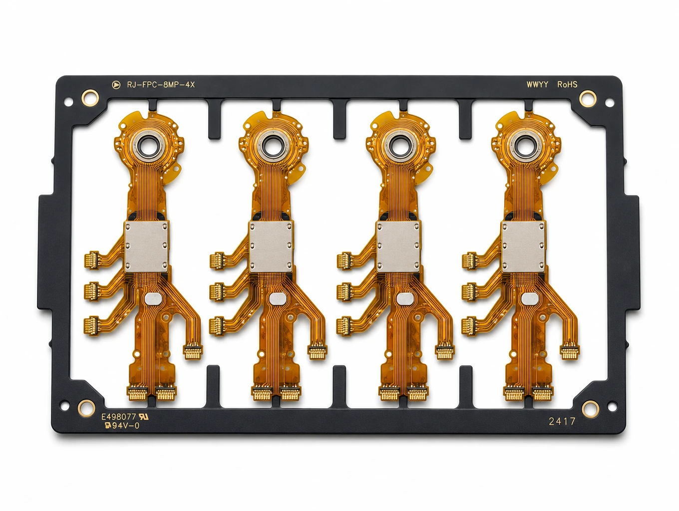
Multi-Branch Humanoid Robotic Joint FPC
Model: TLX-ROB-JNT01
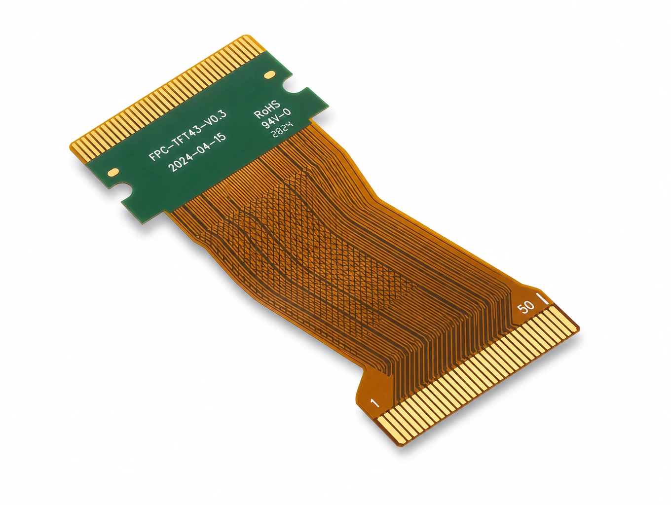
Industrial HMI & TFT-LCD Module FPC
Model: TLX-DFPC-IND05
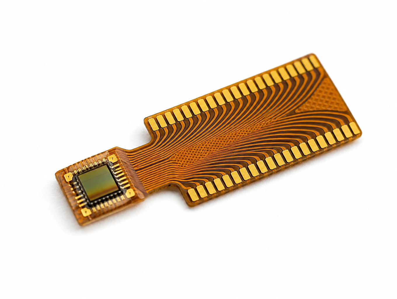
Medical Endoscope Micro-Display FPC
Model: TLX-DFPC-MED06
Related Solutions

RF & Communication FPC Solutions
Custom RF flexible PCB and telecom interconnects for antenna modules, wireless terminals and high-speed communication assemblies. Coordinate materials, signal paths, shielding and connector support with Teleconix before prototype release.
Explore Solutions
Medical Device FPC Solutions
Custom flexible circuits for diagnostic equipment, patient monitoring and compact medical electronics. Discuss routing, signal paths, materials and prototype acceptance with Teleconix before releasing your OEM design.
Explore Solutions
Consumer Electronics & Smart Card FPC Solutions
Custom flexible circuits for smart cards, TWS earbuds and compact wearables. Align routing, stack-up, component interfaces and prototype acceptance with Teleconix before releasing your OEM design.
Explore Solutions RF & Communication FPC Solutions
Custom RF flexible PCB and telecom interconnects for antenna modules, wireless terminals and high-speed communication assemblies. Coordinate materials, signal paths, shielding and connector support with Teleconix before prototype release.
Explore Solutions Medical Device FPC Solutions
Custom flexible circuits for diagnostic equipment, patient monitoring and compact medical electronics. Discuss routing, signal paths, materials and prototype acceptance with Teleconix before releasing your OEM design.
Explore Solutions Consumer Electronics & Smart Card FPC Solutions
Custom flexible circuits for smart cards, TWS earbuds and compact wearables. Align routing, stack-up, component interfaces and prototype acceptance with Teleconix before releasing your OEM design.
Explore SolutionsFrequently Asked Questions
Conclusion: release a reviewed multilayer construction
A multilayer flexible PCB project is ready for sourcing when its layer construction, electrical interfaces, installed route and acceptance plan agree. Establish why extra layers are needed, resolve the supplier’s DFM feedback and carry the approved decisions into one revision-controlled package.
Teleconix can review your intended application and project files so the discussion covers the actual interconnect, quantities and delivery scope. Share your proposed stack-up, connector drawings and installed geometry through the OEM project review process, or contact Teleconix to discuss your multilayer flex PCB requirements. Confirm the construction and service scope for your project before releasing a purchase order.