
Adhesiveless flex PCB: define the material decision first
An adhesiveless flex PCB uses a base laminate in which copper is bonded to the dielectric without a separate base adhesive layer. The term describes the laminate construction. A finished circuit can still contain adhesive in its coverlay, bonding layers or local stiffeners. OEM drawings should identify those materials separately.
The practical question is whether a proposed construction meets the installed thickness, bending, electrical and assembly requirements. Requesting “adhesiveless” without those requirements leaves the supplier to make assumptions about the rest of the stack-up. It also makes quotations difficult to compare.
For example, an optical sensor may need a thin flex route around a housing feature while its connector requires a thicker supported termination. Removing the base adhesive does not resolve both regions automatically. This guide explains how to review that decision, prepare a clear material callout and connect it to prototype evidence. Start with the broader flexible PCB materials guide when the entire material system remains undecided.
Compare base laminates on the same construction boundary
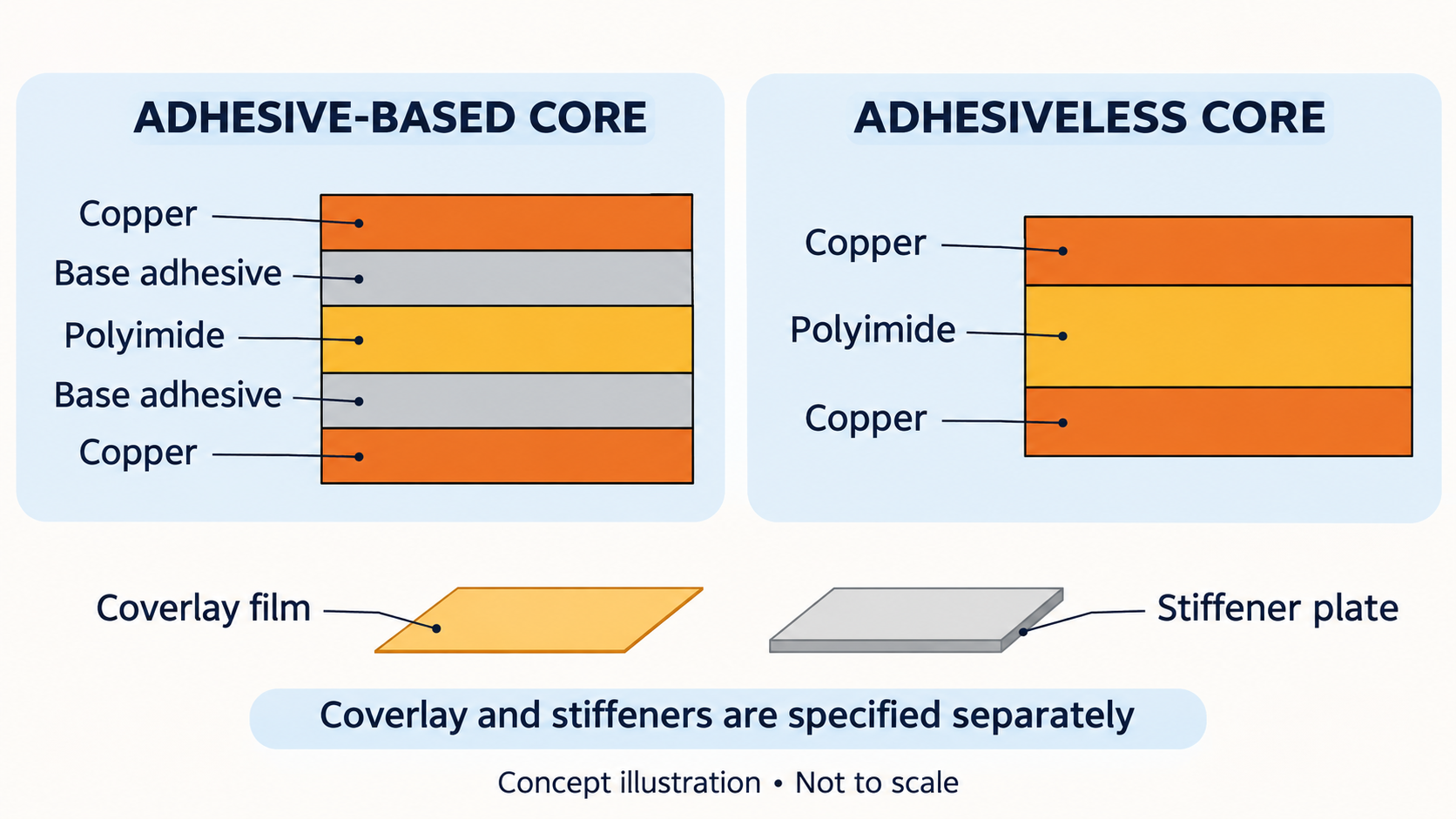
Compare equivalent base cores before comparing complete circuits. An adhesive-based copper-clad laminate includes a separate adhesive between copper and the dielectric film. An adhesiveless core omits that separate layer. Copper, dielectric thickness and the number of conductor sides still need to be specified.
Qnity describes Pyralux AP as an adhesiveless, all-polyimide double-sided laminate. That is a material-family definition, not a complete specification for a finished OEM circuit or a statement about Teleconix material inventory.
| Review item | Adhesive-based core | Adhesiveless core |
|---|---|---|
| Copper-to-film interface | Includes a separate base adhesive | No separate base adhesive layer |
| Copper specification | Specify type and thickness | Specify type and thickness |
| Coverlay and reinforcement | Specify separately | Specify separately |
| OEM acceptance | Verify the finished construction | Verify the finished construction |
Keep the comparison neutral. A familiar adhesive-based construction may meet the application requirements. A thinner core may be useful elsewhere. The selection should follow documented constraints rather than an assumption that one label guarantees a better product.
Map every layer in the finished stack-up
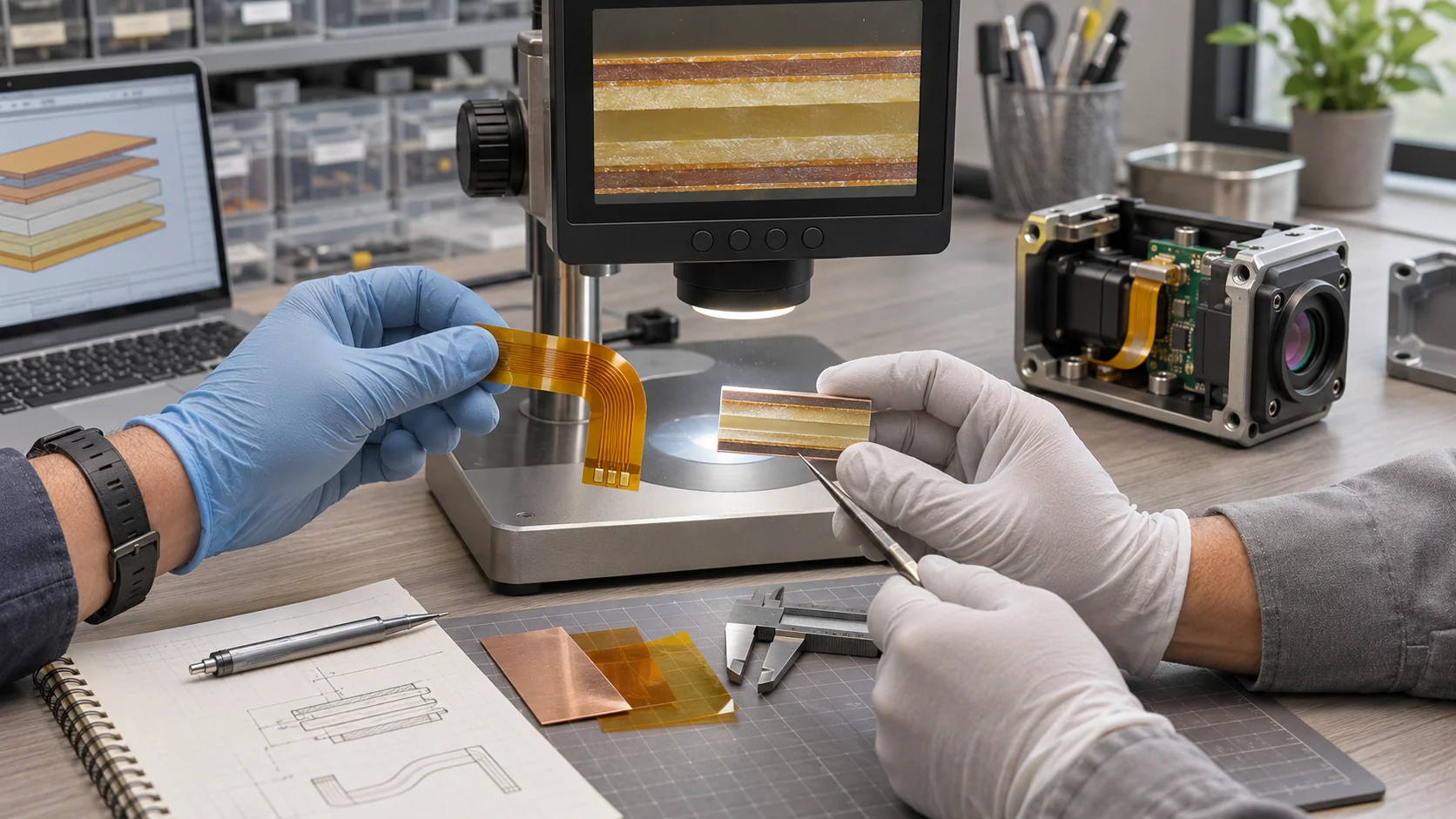
Draw the finished stack from one external surface to the other. Include copper, base dielectric, coverlay film, coverlay adhesive, bonding material and any local reinforcement. Identify which layers continue through the flexing region and which exist only near a connector or component.
For each layer, record a material reference, nominal thickness and applicable finished tolerance. Distinguish starting copper from finished copper where additional processing affects the result. Show separate cross sections for the bend region, plated features and reinforced termination rather than using one headline thickness for the whole part.
A supplier proposal should explain how those cross sections relate to the drawing. If a thickness is still an estimate, identify it as an open item before mechanical release. This prevents an early laminate choice from becoming an accidental final circuit specification.
The flex PCB coverlay guide helps review openings and local coverage. Check the complete layer map before describing a delivered circuit as adhesive-free.
Specify copper independently of the adhesiveless label
State the copper requirements explicitly. “Adhesiveless” does not identify rolled annealed or electrodeposited copper, copper thickness, surface treatment or the finished conductor geometry. These are separate purchasing and engineering decisions that should remain visible in the proposal.
Ask the supplier to identify the offered copper construction and explain its suitability for the intended routing and movement. Record the trace orientation, critical conductor widths and the regions affected by a bend. Review those details together with the dielectric and any additional layers in that region.
For a recurring-motion application, the relevant evidence comes from a representative construction tested under agreed conditions. A material-family name or an unrelated motion result does not establish the operating life of your assembly.
When comparing alternatives, hold the other variables steady where possible. If a proposal changes both the core construction and copper thickness, describe it as a different stack-up. Evaluate its mechanical and electrical effects before interpreting a thickness or price difference as the benefit of removing base adhesive alone.
Review installed bends and recurring motion separately
Define how the circuit moves before approving its construction. An installation bend, occasional service movement and continuous articulation are different conditions. Provide the installed shape, bend direction, available space and the sequence used to place the circuit inside the enclosure.
Altium's rigid-flex design guide discusses material construction and layer count in relation to flexible sections and repeated bending. Apply that guidance through a review of the actual assembly rather than adopting a universal life claim.
Mark the intended active bend region on the drawing. Check nearby vias, conductor transitions, stiffener edges, components and housing features. Confirm that closing the enclosure does not create an unintended crease or transfer movement directly to a termination.
Use the flex PCB bend-radius planning guide to organize the geometry and verification inputs. Agree on a representative test arrangement, environmental conditions and acceptance limits when repeated motion matters. A reduced nominal thickness alone is not a release criterion.
Treat coverlay and stiffener interfaces as local designs
Coverlay and reinforcement can determine the local thickness even when the base core is thin. Review where the coverlay ends, where pads remain exposed and how a stiffener supports insertion or assembly. Document the transition between a supported termination and the flexible route.
Altium's coverlay guidance describes the protective film and adhesive construction used over flex circuitry. Removing a base adhesive layer does not remove the need to account for coverlay adhesive and its openings.
For a connector, use the connector drawing to define the required finished mating thickness and its tolerance. Identify whether that dimension includes the flex core, external coverings, stiffener and bonding material. Check the insertion orientation and exposed contact geometry on the same drawing.
The flexible PCB stiffener guide provides a separate review path for reinforcement. Keep the supported region outside the intended moving section unless the resulting interface has been specifically reviewed and verified.
Review multilayer and rigid-flex bonding separately
An adhesiveless starting core can be part of a multilayer or rigid-flex circuit that uses additional bonding materials. Specify the full lamination construction and distinguish the flexible span from rigid regions and transitions. The starting core does not describe every interface in the finished board.
Identify which conductive layers enter the flexible span, where they terminate and how the structure changes near the rigid section. Review the local finished thickness and physical route rather than relying only on the total layer count used in the rigid region.
Ask the supplier to flag material compatibility, lamination assumptions and construction details that require confirmation. Keep proposed bonding materials and any permitted substitutions within the controlled stack-up document.
The multilayer flexible PCB guide and rigid-flex PCB planning guide address those broader constructions. Use them when the project needs more than a simple core comparison. Do not carry a single-layer thickness assumption into a multilayer quotation without reviewing the added interfaces.
Use the proposed stack-up in electrical calculations
Review electrical requirements against the actual proposed materials and geometry. A change in dielectric arrangement, copper or external covering can change the inputs to a transmission-line model. The word adhesiveless does not establish an impedance value, insertion loss or signal-quality result.
Provide interface information, relevant operating conditions, conductor geometry constraints and the required reference path. Where controlled impedance is necessary, agree on the target, tolerance, modeling assumptions and verification approach before release. Ask which material properties and thicknesses were used in the proposed calculation.
For a compact sensor link, distinguish sensitive analog paths, fast digital edges and power routing. State which requirements are critical and how they will be checked in the assembled system. This makes the material discussion more useful than a general request for a “high-frequency” flex.
The controlled impedance flex PCB guide explains the information needed for that review. Revisit the electrical assumptions whenever an approved material or layer thickness changes.
Confirm assembly and handling requirements
Plan fabrication, storage and assembly as part of the construction review. Record the expected soldering process, assembly sequence, temporary support and handling conditions. Request the applicable material and process guidance rather than creating a universal bake or reflow instruction from the laminate label.
Check whether the flex must remain flat during component placement, whether a carrier is needed and how operators will support the termination. Review local reinforcement and component clearances in the same installed orientation used for mechanical approval.
If a material supplier specifies moisture handling or preparation conditions, incorporate the applicable requirements into the agreed process. Confirm who owns those instructions and how changes are communicated between the circuit fabricator, assembler and OEM.
For assembled products, include the BOM, placement data and assembly drawing in the review package. The FPC assembly guide helps define that scope. An adhesiveless base laminate is one input to the assembly plan; it does not replace process confirmation for the completed construction.
Write a material callout that purchasing can use
A useful callout identifies the proposed construction clearly enough for engineering and purchasing to order the same thing. State the material reference or agreed performance requirements, copper construction, dielectric thickness, number of conductor sides and any allowed alternatives.
For a two-sided circuit, identify whether both sides use the same copper thickness and whether the proposed construction is balanced. Include the coverlay and local stiffener callouts separately. Link each requirement to the relevant drawing region or cross section so a local exception is not applied to the whole circuit.
Use an open-item list when a detail remains undecided. For example, record “supplier to propose connector reinforcement for drawing review” rather than leaving an unexplained blank or allowing an early sample to become the purchasing reference.
Finish with a revision identifier and approval owner. A quotation should identify the proposed material system and its exceptions. If the offered construction differs from the request, review the difference before accepting it as an equivalent.
Compare quotations using the same released assumptions
Compare complete proposals with the same scope. A lower quotation may use a different copper construction, coverlay, reinforcement, inspection plan or assembly allowance. Check those differences before attributing the price to adhesive-based versus adhesiveless material.
Ask each supplier to identify the proposed stack-up, material availability assumptions, quantities and included documentation. Separate prototype work from production quantities and show the items that remain subject to confirmation. If an alternative requires a drawing change, include that review in the comparison.
Keep the commercial discussion connected to the application. A construction that meets the installed requirements with an established supply route may be preferable to one selected solely for a thinner nominal core. There is no universal price premium or saving that applies to every project.
Use the flexible PCB cost guide for the wider cost drivers and the flexible PCB RFQ checklist to prepare comparable manufacturing files. Request confirmation of the offered construction before issuing a purchase order.
Verify a representative prototype before release
Build a verification plan around the risks that motivated the material selection. If the reason was enclosure clearance, measure and inspect the finished assembly. If it was recurring movement or an electrical interface, define a corresponding test using the proposed construction.
| Decision | Evidence to agree |
|---|---|
| Installed thickness | Defined measurement locations, tolerance and assembled clearance |
| Connector interface | Finished mating thickness, insertion and retention checks |
| Repeated motion | Representative geometry, environment, duration and acceptance limits |
| Electrical behavior | Continuity/isolation and agreed application-specific verification |
| Construction identity | Material and drawing revisions connected to the tested sample |
Assign an owner, method and acceptance criterion to each check. Preserve the sample configuration and any temporary substitutions. Results from a different enclosure, copper construction or reinforcement remain conditional until their relevance is reviewed. The flexible PCB prototype guide helps organize those records before production release.
Control substitutions and construction changes
Define which changes require OEM approval before the first production order. A supplier's alternative laminate, copper construction, coverlay adhesive or stiffener bond may affect the assumptions used for mechanical or electrical verification. Similar nominal thickness does not establish equivalence by itself.
Keep an approved stack-up with material references and revision history. Connect delivered lots to the agreed drawing and the inspection records required by the purchase specification. State the documentation you need during the quotation stage so it is included in the offered scope.
When evaluating a substitution, identify the changed layers, affected drawing regions and tests that support acceptance. Record the reason for approval and any limits on its use. An emergency prototype deviation should not silently become the default production construction.
This review also helps purchasing interpret supplier proposals consistently. Use the same controlled identifiers in engineering drawings, purchase descriptions and acceptance records so all teams can tell which construction was ordered and which one was tested.
Choose the next review from the actual application
Use the application to decide which questions need priority. A compact display link may be constrained by connector thickness and installed routing. A moving camera module may need a more detailed motion review. A communication link may require a defined electrical model and measurement plan.
The product and solution references below are starting points for those discussions. They do not establish that a listed example uses a particular adhesiveless laminate. Ask which construction can be proposed for your drawings and what evidence will support the intended use.
Bring the enclosure route, interface requirements and current stack-up to the review. Identify the reason for considering adhesiveless material, the constraints that are fixed and the items still open. This helps both teams compare practical alternatives.
For the wider design release, use the flexible PCB design guidelines. Keep the base-core decision connected to the complete assembly and its acceptance plan.
Related Products
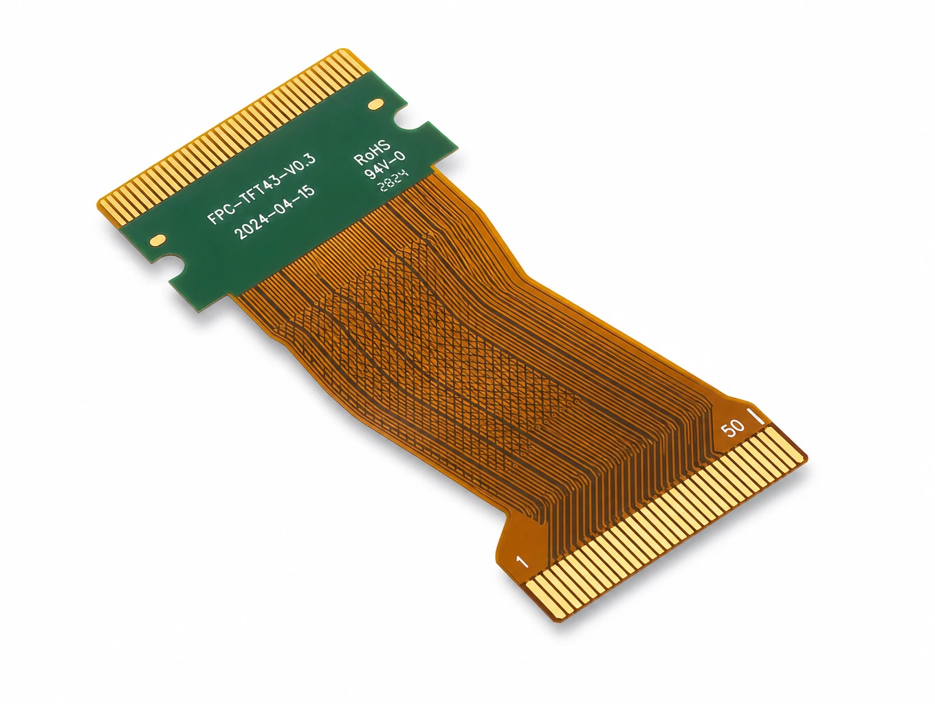
Industrial HMI & TFT-LCD Module FPC
Model: TLX-DFPC-IND05
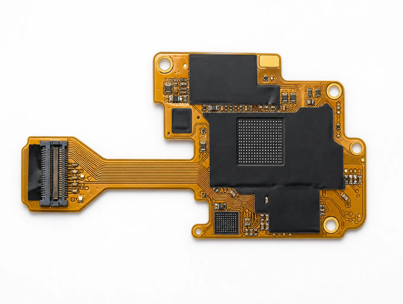
High-Speed ADAS Multi-Camera SerDes FPC
Model: TLX-AUTO-ADAS02
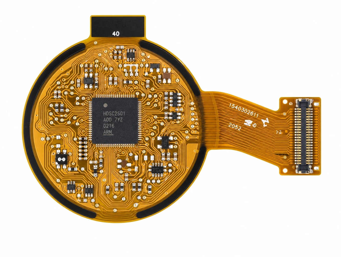
Wearable Smartwatch & Round AMOLED FPC
Model: TLX-DFPC-WEAR04
Related Solutions

Display FPC
Display FPC products for OLED, AMOLED, micro-LED and TFT-LCD modules in handheld, wearable, automotive and industrial devices. Review the display interface, connector and installed flex shape together.
Explore Solutions
AI & Robotics & Special Industrial FPC
Flexible circuits for robotic joints, vision sensors, actuators and industrial interfaces. Match the circuit route to the motion, electrical connections and enclosure of your machine.
Explore Solutions
RF & Communication FPC Solutions
Custom RF flexible PCB and telecom interconnects for antenna modules, wireless terminals and high-speed communication assemblies. Coordinate materials, signal paths, shielding and connector support with Teleconix before prototype release.
Explore Solutions Display FPC
Display FPC products for OLED, AMOLED, micro-LED and TFT-LCD modules in handheld, wearable, automotive and industrial devices. Review the display interface, connector and installed flex shape together.
Explore Solutions AI & Robotics & Special Industrial FPC
Flexible circuits for robotic joints, vision sensors, actuators and industrial interfaces. Match the circuit route to the motion, electrical connections and enclosure of your machine.
Explore Solutions RF & Communication FPC Solutions
Custom RF flexible PCB and telecom interconnects for antenna modules, wireless terminals and high-speed communication assemblies. Coordinate materials, signal paths, shielding and connector support with Teleconix before prototype release.
Explore SolutionsFrequently Asked Questions
Release an agreed construction, then order the build
An adhesiveless flex PCB decision is useful when it resolves a documented OEM requirement. Define the base core, then account for copper, coverlay, bonding materials and reinforcement across the finished circuit. Confirm the installed shape and verify the assumptions that matter to the application.
Prepare the current drawings, proposed stack-up and unresolved questions, then discuss your flex PCB project with Teleconix. Agree on the material proposal, prototype scope and acceptance records before treating the construction as released for production.