
Consumer electronics FPC planning starts with installed function
A consumer electronics FPC is a flexible printed circuit that connects or carries electronic functions inside a consumer device. The useful starting point is the installed assembly: which modules it connects, how it reaches them, and what evidence will establish acceptable operation. A thin outline alone does not describe a buildable interconnect.
For an OEM developing earbuds, a smartwatch or a smart card, the challenge is often shared ownership. Electrical engineering controls the interface, mechanical engineering controls the enclosure, and purchasing needs a repeatable delivered specification. Bring those decisions together before requesting a production quotation. Otherwise, a supplier may price a flat circuit while the product team expects a fitted and verified assembly.
This guide connects wearable, compact audio and smart-card requirements to practical design inputs and sample checks. Use the consumer and smart card FPC product category to explore relevant configurations. Confirm each proposed construction and manufacturing capability against your project; a product family name cannot establish service life, environmental suitability or finished-device approval.
Separate the interconnect from the complete device architecture
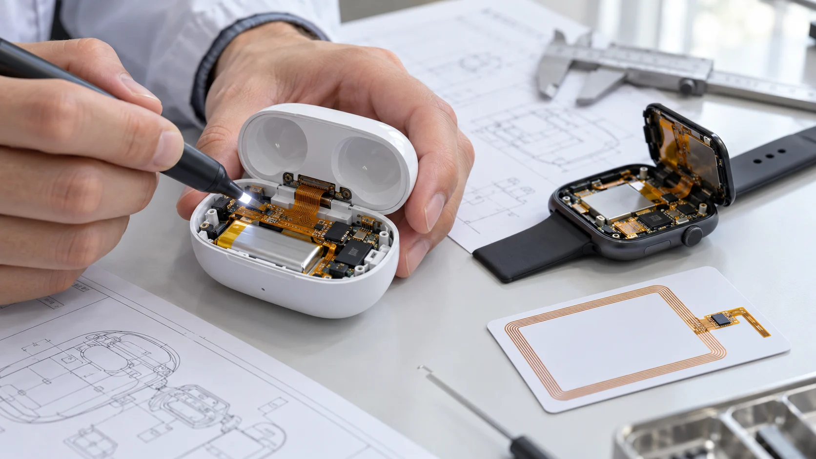
Identify whether the FPC is a passive connection, a populated assembly, an antenna inlay or a combination of these functions. An earbud charging-case interconnect may carry power, indicators and sensor signals. A smart card FPC may connect a fingerprint sensor or display to other electronics. Those uses need different drawings and verification responsibilities.
List the delivered boundary explicitly. State whether the quotation includes components, connector installation, stiffeners, adhesives, bonding, programming, test fixtures or enclosure installation. Assign customer-supplied parts and downstream assembly work. This prevents two commercially similar proposals from concealing substantially different engineering tasks.
Where a standard cable is also an option, compare interface and routing requirements before choosing custom circuitry. The FPC versus FFC selection guide explains the architecture questions. A custom outline is useful when the device needs it, but it also creates drawing, tooling and change-control responsibilities that should appear in the programme plan.
Build an application matrix before selecting a stack-up
Use one table to connect each application to its unresolved decisions and intended checks. Include the device revision and the owner who can approve each interface. This turns a broad request for a wearable flexible PCB into an actionable conversation about construction, installation and evidence.
For example, a watch sensor tail and an NFC card coil can share a material family while having very different design objectives. Do not combine them under a single thickness or bend requirement. Ask the supplier to identify the assumptions behind each proposed configuration and record the response with the quotation.
| Application | Decisions to define | Installed verification |
|---|---|---|
| TWS earbuds and charging cases | Charging contacts, sensors, hinge route and installation access. | Mating fit, supported routing and device operation after assembly. |
| Watches and compact wearables | Sensor position, enclosure datums, display connection and service access. | Installed fit, connector retention and required sensing functions. |
| Smart-card sensor or display connection | Card construction, local thickness, bonding process and module location. | Connection integrity and operation after the agreed card assembly process. |
| NFC antenna inlays | Selected IC, coil layout, nearby materials and tuning responsibilities. | Electrical characterisation and contactless operation in the final construction. |
| Smart-home controls and keypads | Switch or sensor interface, mounting, enclosure edges and handling. | Input operation, fit and the specified handling or environmental checks. |
Keep this matrix with the approved file set. A change to an enclosure, sensor or adhesive can reopen a decision even when the copper artwork is unchanged. Update the relevant checks rather than treating the earlier sample result as permanent approval.
Give wearable FPC routing a three-dimensional definition
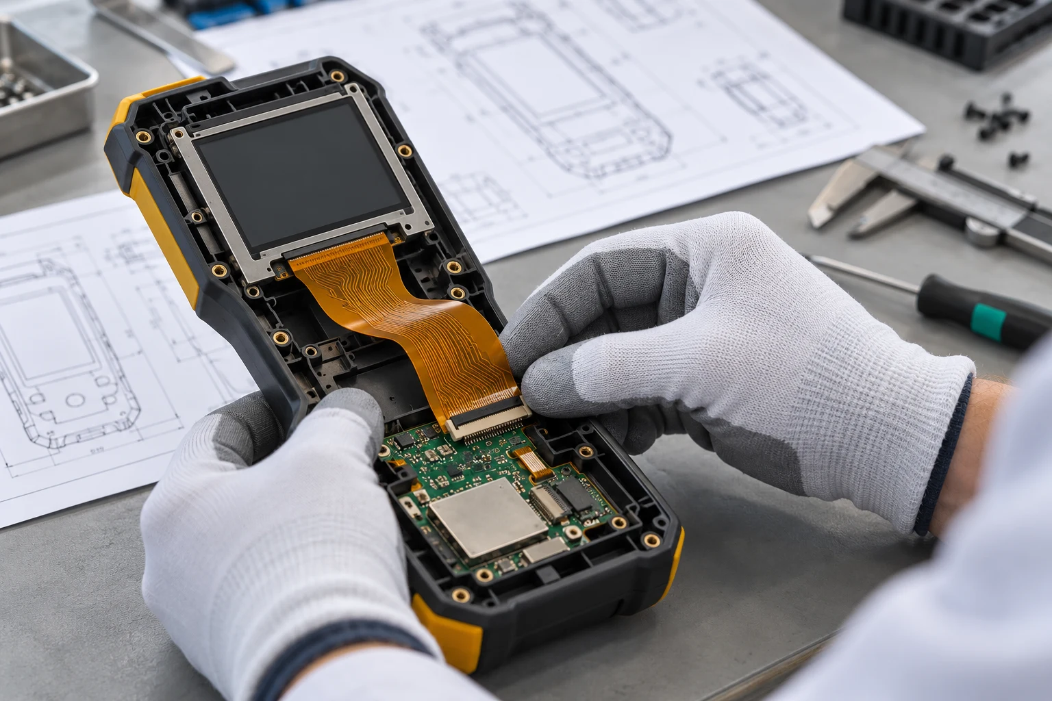
A wearable device FPC needs a route through the actual enclosure, including component heights, fasteners, sensor windows and the closing sequence. Show the final position and the intermediate positions used during assembly. A circuit may fit when the lid is open but become trapped or stretched when the housing closes.
Identify datums and tolerance accumulation between connected parts. Provide enough information to review where slack is accommodated and which regions must remain clear. Avoid relying on a flat artwork view to describe a curved watch housing or a small ring assembly. Use a mechanical mockup to check insertion direction, tool access and retention before committing to production-intent samples.
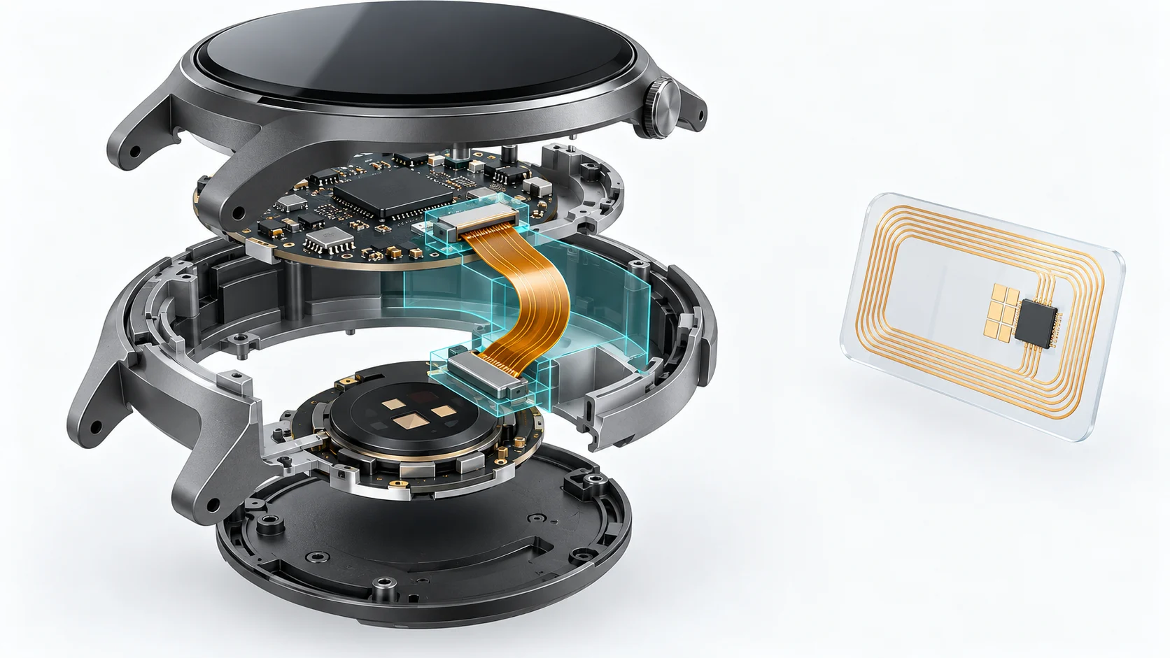
The illustration below highlights a supported connector region and a reserved route inside a compact wearable. It is a concept for reviewing space and support, not a manufacturing drawing. Define the actual clearances, local stack and acceptance dimensions on controlled project drawings; they should reflect the selected parts and assembly method.
Distinguish installation folds from recurring motion
Classify each flexible region by its duty. A one-time installation fold, a service opening and a hinge that moves during normal use should not inherit the same requirement. Describe the motion path, available space, movement rate and expected exposure sequence where recurring movement exists. Identify what stays fixed and what travels.
Use the static and dynamic flex bend guide to structure the discussion. Bend suitability depends on the complete construction and installed geometry. Do not assign a universal radius or lifetime from the word flexible, or assume that a thin circuit will tolerate any fold. The supplier needs the actual application conditions to propose a reviewable construction.
For an earbud charging case, check whether the FPC crosses the lid hinge or stays entirely in the fixed housing. Review contact with edges and adjacent parts throughout the defined travel. Establish sample observations and acceptance criteria for that duty, including connection checks after movement. Keep the test configuration representative of the production supports and assembly sequence.
Control connector tails and local reinforcement
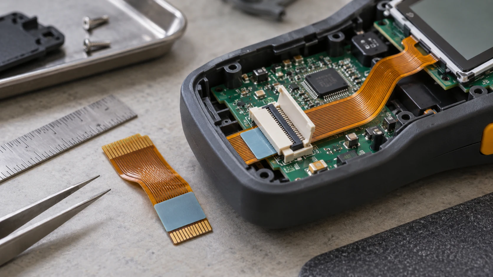
Specify the complete mating connector part number, contact side, insertion depth and finished tail requirements. Pitch alone does not establish compatibility. Include the effect of protective layers, plating, stiffener and adhesive in the finished construction review. Confirm that the connector latch can be operated after neighbouring parts are installed.
The flexible PCB stiffener checklist helps define support boundaries. Review where the reinforcement ends and how the flexible span leaves that support. A local step can create an unintended hinge if the enclosure forces bending at the edge. Check the installed route with representative mating parts rather than accepting only nominal dimensions.
Small assemblies also need a handling plan. State how operators grip, insert and retain the tail without loading a populated region or damaging exposed contacts. Define inspection access and permitted rework. If the circuit is bonded instead of connectorised, document the mating surface, process owner and evidence required to release that connection.
Specify materials as a complete assembled construction
Compare conductor, dielectric, coverlay, finish, reinforcement and adhesive together. Define where each layer starts and stops and which surfaces will be bonded, exposed or contacted. A material designation alone cannot explain local thickness, flexibility, dimensional behaviour or the effect of the assembly process.
Use the flexible PCB materials review guide for the broader selection questions. For compact consumer hardware, add local stack limits around sensors, connectors and enclosure seals. Ask the supplier to state proposed alternatives and the change-control process. A material substitution can require renewed fit, assembly or functional checks even when its nominal thickness is similar.
For a laminated smart-card assembly, identify the actual surrounding materials and process conditions supplied by the card manufacturer. Agree which party evaluates the complete construction after lamination. Neither a bare-circuit continuity report nor an isolated substrate property demonstrates finished-card suitability. Keep the approved construction and process assumptions with the sample report.
Separate smart-card interconnect and antenna requirements
A smart card FPC can serve a sensor, display, chip connection or antenna function. Define these functions separately and identify their electrical relationship. The outline and local thickness must be coordinated with the complete card construction, including component pockets, attachment features and surrounding layers.
Infineon’s Card Coil Design Guide covers coil design and characterisation for its specified contactless memory products. It calls for measurement to verify the particular design. For an OEM review, this supports assigning coil characterisation to the selected IC and finished construction rather than treating an antenna-shaped trace as a qualified contactless system.
Record who owns tuning, bonding and final contactless testing. Keep payment-system approval, security evaluation and any required card qualification with the responsible product programme. Fabricating an FPC does not establish those approvals. Request applicable evidence for the actual delivered scope and avoid transferring a chip or another card’s certification to a new assembly.
Review NFC and high-speed interfaces in their actual surroundings
Identify the selected interface and use its component documentation. A sensor connection, display channel and NFC coil do not share one universal electrical target. State reference paths, connector transitions and any controlled geometry required by the actual design. Separate antenna tuning from transmission-line impedance control.
NXP’s PN5190 antenna design guide, written for an NFC reader device, explains that the housing, mounting and nearby metal influence antenna behaviour. This illustrates why the mechanical environment belongs in an NFC review; its reader-specific circuitry and settings are not a recipe for an unrelated smart card or wearable.
For a consumer device, provide the final enclosure materials, nearby battery or shielding location and proposed assembly arrangement to the responsible antenna designer. Agree checks in that representative configuration. Where a display or data link requires controlled geometry, use the controlled impedance flex PCB guide and the selected interface specification to define the separate channel requirements.
Plan populated assembly and joining before closing the enclosure
Decide whether the supplier delivers a bare FPC or a populated assembly. For assembly, supply the controlled BOM, placement data, polarity information and relevant drawings. Identify customer-supplied components, substitutions and any process restrictions. Small size does not remove the need for a clear delivered scope.
Review support during component placement, joining, inspection and handling. Define which local areas must remain flat and how components are protected while flexible spans are routed. Coordinate adhesive application and enclosure assembly so that a later operation does not contaminate contacts or prevent inspection of an earlier joint.
Agree test access and repair limits before layout release. A contact pad hidden under the final cover may be useful during manufacture but unavailable after installation. Assign each check to the stage where it can be performed reliably. Preserve assembly observations from samples and turn accepted handling methods into the controlled build instructions.
Define environmental exposure at the circuit location
Describe conditions where the FPC sits, including assembly heat, humidity, cleaning agents, sweat exposure, vibration and user handling where relevant. Distinguish a protected internal circuit from an interface exposed through a device opening. The enclosure design and sealing approach determine which conditions reach the assembly.
For a smart ring flexible PCB or smart watch FPC, identify what the product specification requires and which tests apply to the finished device. Do not infer a device water-resistance rating from the flex material or a coating description. Include seals, joints and the production assembly method in the appropriate validation plan.
Choose verification conditions with the responsible product team and record their source. State the sample configuration, operating state and observations required before and after exposure. Avoid generic claims about unlimited bending or guaranteed durability. Useful purchasing evidence connects the requested environment to a documented construction, agreed test sequence and identifiable sample results.
Verify prototypes after representative installation
A flat bare-board electrical test can find certain circuit defects, but it cannot establish every installed function. Build a prototype plan that includes dimensional checks, mating fit, route inspection and the relevant electrical or functional checks after assembly. Identify the failure mechanism each check is intended to reveal.
For example, verify that a wearable sensor remains positioned correctly, a charging-case connection stays engaged and a card assembly still performs its required function after the agreed manufacturing sequence. Define repeatable fixtures, observations and acceptance conditions. The test owner should distinguish a manufacturing sample from a sample intended for environmental or product qualification.
Use the flexible PCB prototype validation guide to connect sample purpose to release evidence. Retain photographs, configuration records and deviations with the results. When an enclosure or adhesive changes, review which checks need repeating. A pass on an earlier configuration should not silently release a different installed assembly.
Compare quotations using the same delivered scope
Purchasing should compare equivalent quantities, construction revisions and delivery boundaries. Separate one-time tooling, sample work, components, assembly, inspection, testing and documentation where applicable. Identify exclusions such as antenna tuning, enclosure installation, firmware work or final product certification. A lower bare-board price can move costs elsewhere in the build.
Review yield and service assumptions with engineering. Ask how the proposed design will be assembled, inspected and replaced if a connected module fails. A permanently bonded flex can change repair scope compared with a removable connection. Evaluate those consequences against the actual product plan rather than claiming automatic savings from fewer parts.
Request current quality and capability evidence for the relevant site, process and proposed scope when it is required by procurement. Keep evidence-based findings separate from marketing statements. Approve the technical construction and acceptance plan alongside the commercial proposal so that a later price negotiation does not become an unreviewed specification change.
Release a revision-controlled consumer electronics FPC package
The RFQ package should contain circuit data, drill and outline information, the proposed stack-up, local thickness requirements, connector drawings and installed mechanical views. Add the BOM and assembly data for populated circuits. State sample purpose, quantities, environmental requirements and the requested inspection or validation records.
Use the flexible PCB RFQ file checklist as the common handover structure. Add the application matrix, antenna responsibilities where relevant, assembly sequence and unresolved decisions. Give each open item an owner and identify the build stage it prevents. Ask the supplier to flag assumptions instead of silently filling gaps.
Before production release, reconcile the accepted sample with the controlled files and approved deviations. Confirm the installed route, connector engagement, construction and functional evidence. Use the related product and solution pages below to start the discussion with Teleconix, then close the specification against your particular device and approval requirements.
Related Products
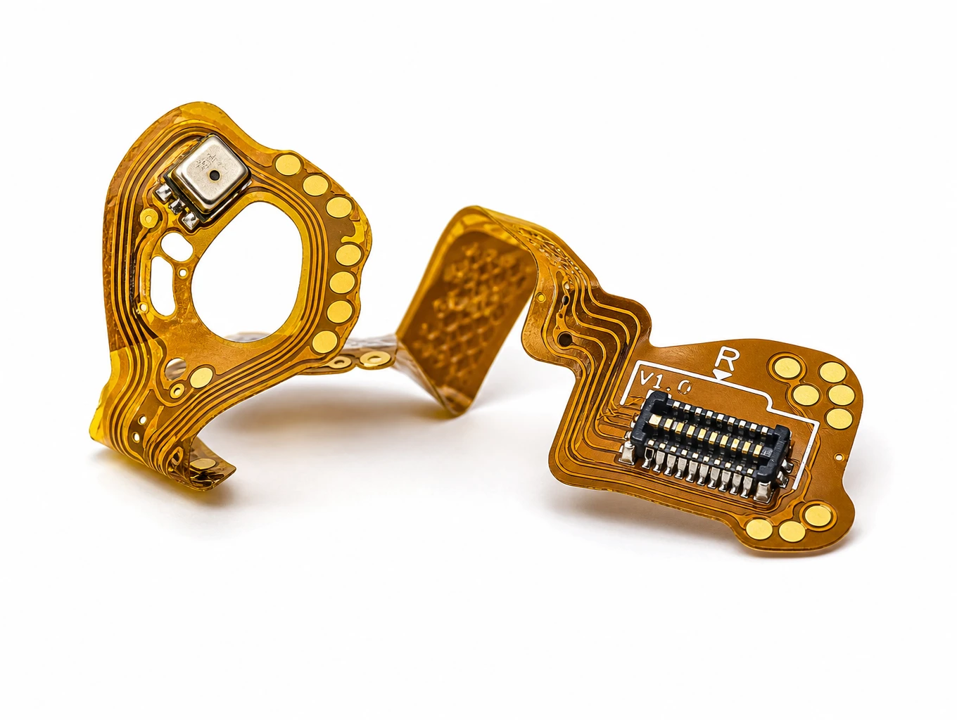
True Wireless Stereo (TWS) Earbud & Charging Case Micro FPC
Model: TLX-CONS-TWS05
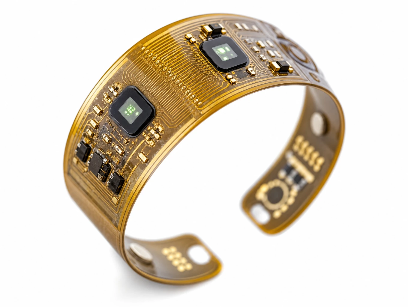
Smart Wearable Health Ring & Biosensor Multi-Flex FPC
Model: TLX-CONS-RING06
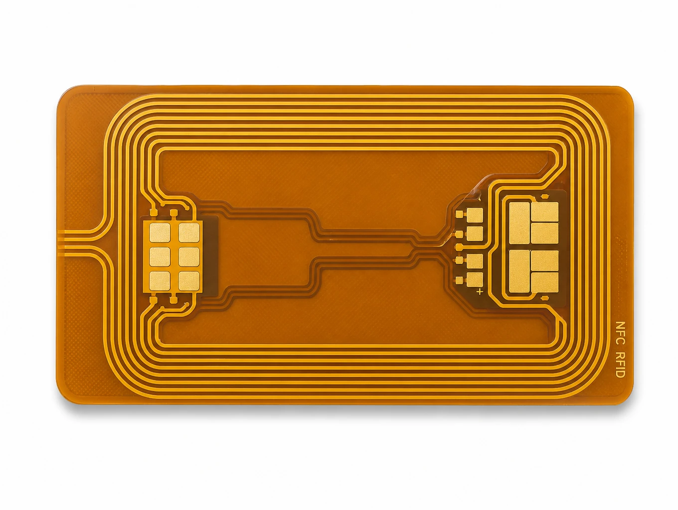
High-Q Precision Etched Dual-Interface NFC Antenna Inlay FPC
Model: TLX-CARD-NFC03
Related Solutions
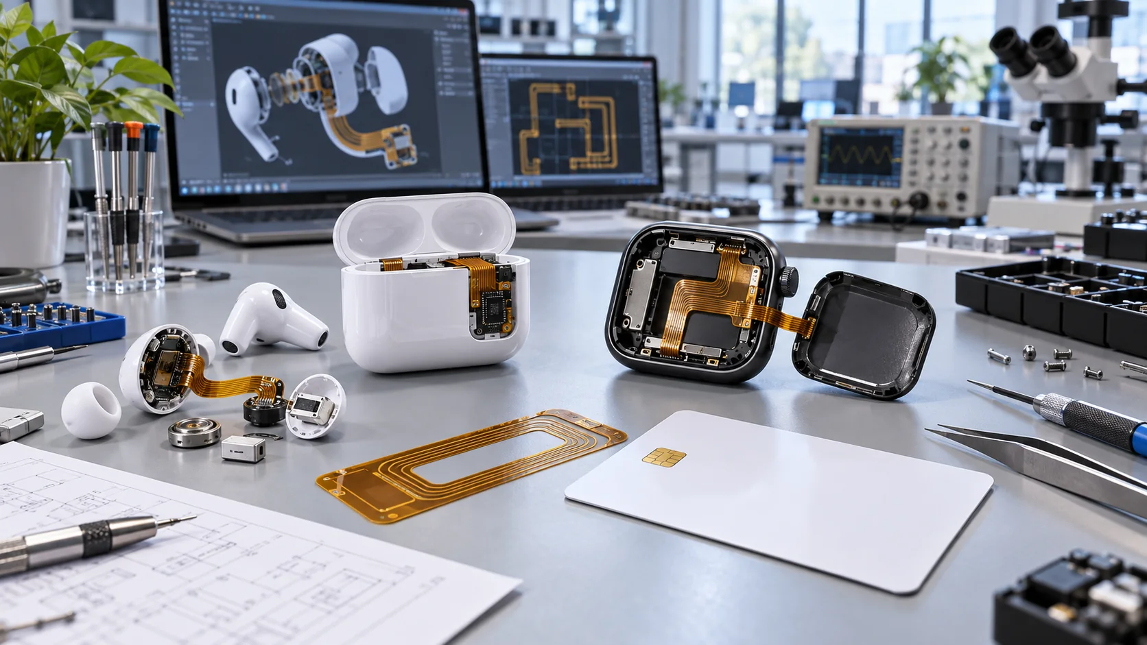
Consumer Electronics & Smart Card FPC Solutions
Custom flexible circuits for smart cards, TWS earbuds and compact wearables. Align routing, stack-up, component interfaces and prototype acceptance with Teleconix before releasing your OEM design.
Explore Solutions
RF & Communication FPC Solutions
Custom RF flexible PCB and telecom interconnects for antenna modules, wireless terminals and high-speed communication assemblies. Coordinate materials, signal paths, shielding and connector support with Teleconix before prototype release.
Explore Solutions
Display FPC
Display FPC products for OLED, AMOLED, micro-LED and TFT-LCD modules in handheld, wearable, automotive and industrial devices. Review the display interface, connector and installed flex shape together.
Explore Solutions Consumer Electronics & Smart Card FPC Solutions
Custom flexible circuits for smart cards, TWS earbuds and compact wearables. Align routing, stack-up, component interfaces and prototype acceptance with Teleconix before releasing your OEM design.
Explore Solutions RF & Communication FPC Solutions
Custom RF flexible PCB and telecom interconnects for antenna modules, wireless terminals and high-speed communication assemblies. Coordinate materials, signal paths, shielding and connector support with Teleconix before prototype release.
Explore Solutions Display FPC
Display FPC products for OLED, AMOLED, micro-LED and TFT-LCD modules in handheld, wearable, automotive and industrial devices. Review the display interface, connector and installed flex shape together.
Explore SolutionsFrequently Asked Questions
Conclusion: release the installed assembly with evidence
A useful consumer electronics FPC specification joins the electrical interface to installed fit and measurable release evidence. Wearables, TWS assemblies and smart cards need clear construction boundaries, supported routes and application-specific checks. Define antenna, bonding and finished-device responsibilities explicitly so each supplier knows what it is being asked to deliver.
Prepare the application matrix, controlled drawings and prototype acceptance plan before comparing production proposals. Discuss your consumer electronics FPC project with Teleconix and share the intended device, assembly scope and required evidence for a focused engineering review.